Lab 3 - EE 421L 

Authored by Ja Manipon
maniponj@unlv.nevada.edu
9/20/16
Lab 3 Design Files

Pre-Lab


Post-Lab

This lab will focus on the layout of the 10-bit DAC you designed and simulated in Lab 2

Ensure that your html lab report includes your name and email address at the beginning of the report (the top of the webpage).
When finished backup your work (webpages and design directory).

N-Well Layout of 10K resistor

Layout and Extracted
Description
http://cmosedu.com/jbaker/courses/ee421L/f16/students/maniponj/lab3/R_N_Well_10K.png
http://cmosedu.com/jbaker/courses/ee421L/f16/students/maniponj/lab3/R_N_Well_10k_Extracted.png
This is my design of a 10K N-Well Resistor. In order to calculate the dimensions of this N-Well, I used the formula R = R(per Square)*(L/W). The minimum width for this design is 3.6um but I bumped it up to 4.5um and added two contacts onto the Ntaps. I plugged the 4.5um into the formula as well as the 800 Ohms per square and rearranged some of the variables to calculate the Length (L = (R*W)/R(Per Square))

L = (10K*4.5u)/800
L = 56.25um

This is how I calculated the length of the N-Well. In the tutorial, it asks you to put in a length of 56um however 56um does not land in the .15um grid per the DRC. So I had to add the .1um in order to make it land on the grid. 56.25um would also work since 56.25/.15 = 375.


DAC Layout with 10K N-Well Resistor

Layout and Extracted
DAC Inputs and Outputs
Description
http://cmosedu.com/jbaker/courses/ee421L/f16/students/maniponj/lab3/DAC_Layout.png    http://cmosedu.com/jbaker/courses/ee421L/f16/students/maniponj/lab3/DAC_Extracted.png
http://cmosedu.com/jbaker/courses/ee421L/f16/students/maniponj/lab3/DAC_Pins_2.pnghttp://cmosedu.com/jbaker/courses/ee421L/f16/students/maniponj/lab3/DAC_Pins_1.png
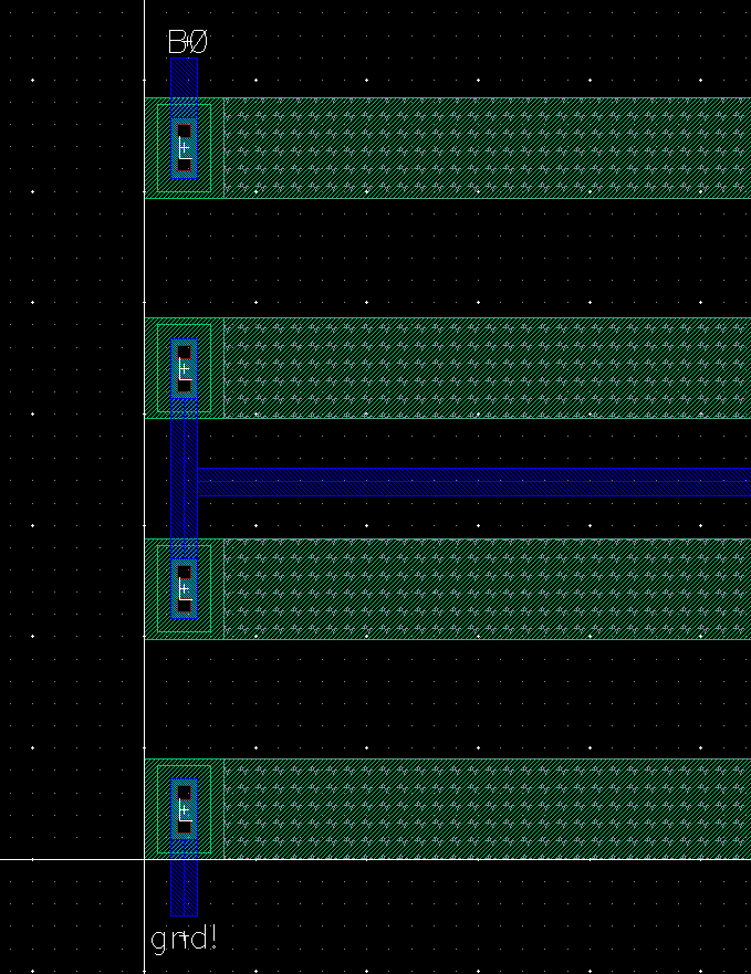
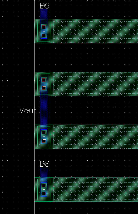
I based the layout on the previous schematic that was created from the previous lab. The resistor that is being used is the one I created going through Tutorial 1. The schematic had 31 resistors in total, four resistors for B0 and three resistors for the rest of the inputs.  First I started with B0 adding the four resistors according to the schematic, then I copied the first three resistors with an array of 9 to take care of the rest of the inputs. After that, I created the metal1 wire to connect the resistors in parallel like in the schematic and copied the wire 9 times to connect the rest of the resistors.Once I completed copying and pasting the metals and resistors, I DRC'd and Extracted the layout for LVS.


DRC and LVS of DAC Layout

DRC and LVS
Schematic Used for the LVS
http://cmosedu.com/jbaker/courses/ee421L/f16/students/maniponj/lab3/DAC_DRC.pnghttp://cmosedu.com/jbaker/courses/ee421L/f16/students/maniponj/lab3/DAC_LVS.png
http://cmosedu.com/jbaker/courses/ee421L/f16/students/maniponj/lab2/10BitDAC_Schematic.JPG
Description
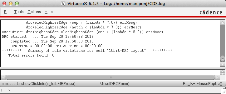
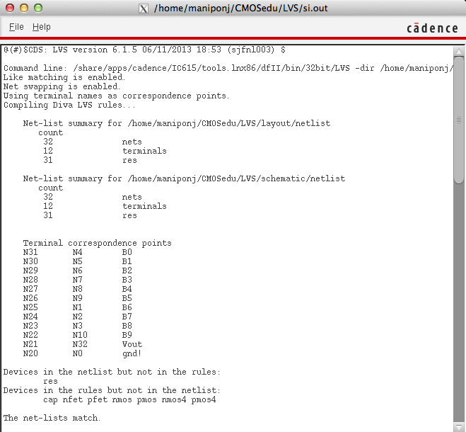
After I ran the DRC on the layout with no errors, I extracted the layout and ran the LVS with the schematic that was created in the previous lab. Net-lists matched and the image above is output from the LVS

Extracted Simulation vs. Schematic Simulation

To run extracted simulation I click on the setup tab in ADE L and click on environment. Then on the top text field I added the word 'extracted' before schematic so it would pick up the extracted view instead of schematic.
When I run all my simulations now, I get this in the log file
http://cmosedu.com/jbaker/courses/ee421L/f16/students/maniponj/lab3/Extracted_Simulation.PNG
SchematicExtractedSimulation
http://cmosedu.com/jbaker/courses/ee421L/f16/students/maniponj/lab2/Simulation_sim2_ideal_ADC_DAC.JPGhttp://cmosedu.com/jbaker/courses/ee421L/f16/students/maniponj/lab3/Extracted_Simulation_Ideal_ADC_DAC.PNGSimulation of Ideal ADC to My DAC
http://cmosedu.com/jbaker/courses/ee421L/f16/students/maniponj/lab2/Cap_Load_simulation.JPGhttp://cmosedu.com/jbaker/courses/ee421L/f16/students/maniponj/lab3/Extracted_Simulation_10Bit_DAC.PNGSimulation of my 10Bit DAC with everything grounded except for B9 with a 10pF load
http://cmosedu.com/jbaker/courses/ee421L/f16/students/maniponj/lab2/R_simulation_sim2_ideal_ADC_DAC.JPGhttp://cmosedu.com/jbaker/courses/ee421L/f16/students/maniponj/lab3/Extracted_R_Simulation_Ideal_ADC_DAC.PNGSimulation adding a 10K resistor as the load
http://cmosedu.com/jbaker/courses/ee421L/f16/students/maniponj/lab2/C_simulation_sim2_ideal_ADC_DAC.JPGhttp://cmosedu.com/jbaker/courses/ee421L/f16/students/maniponj/lab3/Extracted_C_Simulation_Ideal_ADC_DAC.PNGSimulation adding a 10pF capacitor as the load
http://cmosedu.com/jbaker/courses/ee421L/f16/students/maniponj/lab2/RC_simulation_sim2_ideal_ADC_DAC.JPGhttp://cmosedu.com/jbaker/courses/ee421L/f16/students/maniponj/lab3/Extracted_RC_Simulation_Ideal_ADC_DAC.PNGSimulation adding a 10K Resistor || 10pF Capacitor as the loads.

Return to EE 421 Labs