Lab 2 - EE 421L 

Authored by Ja Manipon

maniponj@unlv.nevada.edu

9/14/2016

Pre-lab work


 I backed up all images and files on my local and Google Drive
LocalCloud
http://cmosedu.com/jbaker/courses/ee421L/f16/students/maniponj/lab2/backup.JPGhttp://cmosedu.com/jbaker/courses/ee421L/f16/students/maniponj/lab2/cloud.JPG

Ideal ADC to DAC Backing up Files

Once I added my zip files and defined my library for lab 2, I went into the library and opened up the schematic as well as run the simulation and these are the resulting images below
SchematicSimulationDescription
http://cmosedu.com/jbaker/courses/ee421L/f16/students/maniponj/lab2/Ideal_ADC_DAC.JPGhttp://cmosedu.com/jbaker/courses/ee421L/f16/students/maniponj/lab2/Ideal_ADC_DAC_simulation.JPGThe purpose of the ADC is to convert Analog Signal into a Digital Signal and the DAC is to convert Digital Signal into Analog Signal. The purpose of the DAC is to imitate the analog signal since computers cannot grasp the infinite amount of points an analog signal can give. When the signal goes through the DAC, the output looks like a staircase as shown to the side. The amount of steps is determined by how many bits the DAC contains.  The more bits and the more precise it is and the more it looks like the original Analog Signal.
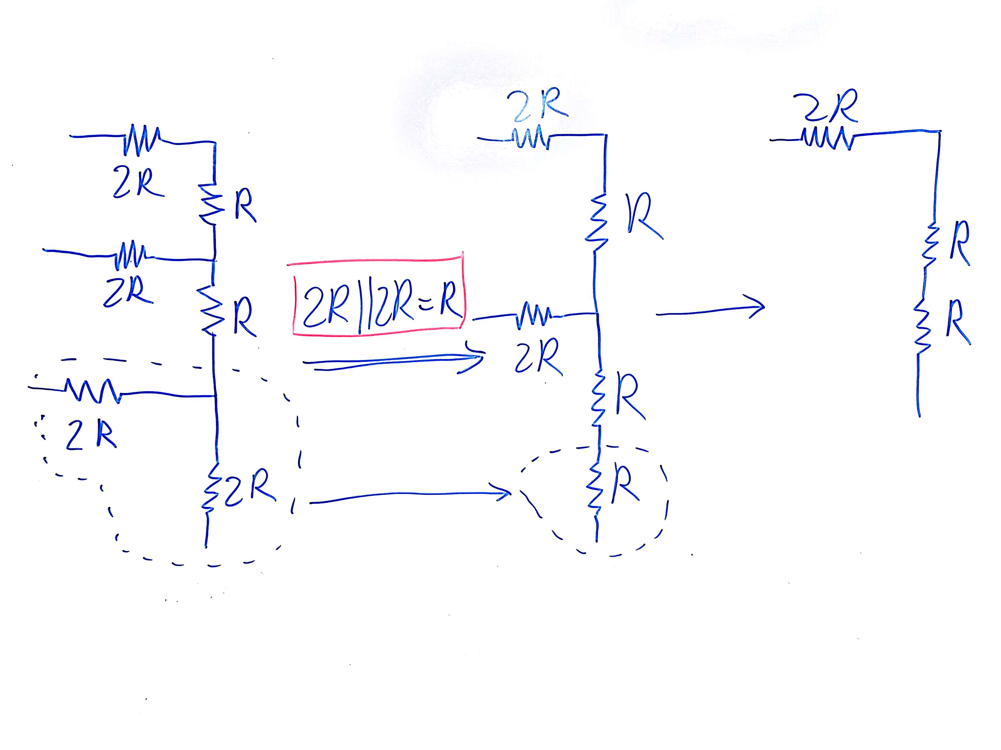
Calculating LSB

1 LSB  = VDD/2^n


Post-Lab:

Design of a 10-Bit Digital-to-Analog Converter (DAC) Schematic

Determining the Output Resistance of the DAC

Visual of DAC Output Resistance
Explanation

http://cmosedu.com/jbaker/courses/ee421L/f16/students/maniponj/lab2/DACRes.jpg

With how the DAC is arranged with a bunch of resistors in series and parallel you can calculate the output resitance to be R. The image to the left shows a basic DAC with 3 Bits. As shown in the image when calculating the output Resistance, which should be R, shows that the LSB has 2R || 2R. This would result it being R. The next step shows R is in series with R making it 2R thus repeating the process of 2R || 2R. Once it reaches the MSB, the result would be R. This can be applied to a DAC with n-amount of bits.

((((2R || 2R) + R) || 2R) + R) || 2R) = R

Schematic and Symbol of DAC

SchematicSymbolDescription

http://cmosedu.com/jbaker/courses/ee421L/f16/students/maniponj/lab2/10BitDAC_Schematic.JPG

http://cmosedu.com/jbaker/courses/ee421L/f16/students/maniponj/lab2/10BitDAC_Symbol.JPGI created the schematic for the DAC based on the schematic of resistors that was given in the prelab and that is shown to the left. Once I finished building the schematic I went into Create->Cellview and created a symbol. I delated all the uneccesary lines for the symbol thus creating the symbol to the left as well..

Grounding the DAC symbol except for B9 and adding 10pF capacitor load

SchematicSimulationDescription
http://cmosedu.com/jbaker/courses/ee421L/f16/students/maniponj/lab2/Cap_Load.JPGhttp://cmosedu.com/jbaker/courses/ee421L/f16/students/maniponj/lab2/Cap_Load_simulation.JPG
Adding the capacitor creates a delay of roughly 70ns. This can be estimated by Td = 0.7RC --> 0.7(10K)(10p) = 70ns
 

Replacing Ideal DAC with own DAC

New SchematicSimulationDescription
http://cmosedu.com/jbaker/courses/ee421L/f16/students/maniponj/lab2/sim2_ideal_ADC_DAC.JPGhttp://cmosedu.com/jbaker/courses/ee421L/f16/students/maniponj/lab2/Simulation_sim2_ideal_ADC_DAC.JPGOnce I replaced the Ideal DAC with my own design, the simulation comes out very similar to the original schematic. The steps are not as refined as the ideal but still 

Adding Different Loads

SchematicSimulationDescription
10K Resistor
http://cmosedu.com/jbaker/courses/ee421L/f16/students/maniponj/lab2/R_sim2_ideal_ADC_DAC.JPG
http://cmosedu.com/jbaker/courses/ee421L/f16/students/maniponj/lab2/R_simulation_sim2_ideal_ADC_DAC.JPGWhen adding a 10K resistor as the load, the sine wave follows the same trend however the voltage is about half the input voltage. Adding this 10K resistor turns the DAC into a voltage divider since we determined the output resistance is 10K and Vout = Vin(10K/(10K+10K)) will give 1/2Vin.
10pF Capacitor
http://cmosedu.com/jbaker/courses/ee421L/f16/students/maniponj/lab2/C_sim2_ideal_ADC_DAC.JPG
http://cmosedu.com/jbaker/courses/ee421L/f16/students/maniponj/lab2/C_simulation_sim2_ideal_ADC_DAC.JPGWhen adding a 10pF capacitor, there is a loss of amplitude as well as a delay of 75ns
10K Resistor || 10pF Capacitor
http://cmosedu.com/jbaker/courses/ee421L/f16/students/maniponj/lab2/RC_sim2_ideal_ADC_DAC.JPG
http://cmosedu.com/jbaker/courses/ee421L/f16/students/maniponj/lab2/RC_simulation_sim2_ideal_ADC_DAC.JPGAdding a 10pF capacitor and 10K resistor results in the output voltage to have a loss of altitude as well as causing a delay by 50ns.

What happens if the resistance of the switches isn't small compared to R?

This would cause the input to encounter high impedance and causing the voltage that is being inputted not go through the DAC, thus causing some errors in the simulation.


Return to EE 421L Student Lab Reports