Project - ECE 421L
Authored
by Antanasia Jones
jonesa20@unlv.nevada.edu
11/30/16
For the lab project I had to design a circuit that can detect the output 101011 when it appears in a series.
In
the first part of the project I had to design a falling edge D-Flip
Flop (DFF) circuit. The DFF is used to inverter a signal based on
the input signal clock. The DFF uses TGs to provide full logic level on
the outputs. Below are images of the transmission gates (TG) circuits
that were used in the DFF schematic. Below are images of the TGs, that are refered to as Clock1 and Clock2, and
DFF circuits, symbols and layouts. Clock1 is the where the clock of the
PMOS is clock and clock of the NMOS is clock inverse. Clock2 is where
the clock on the PMOS clock inverse and the clock on the NMOs is clock.

Clock circuit 1 schematic

Clock 1 Symbol

Clock 1 Layout

Clock 2 circuit schematic

Clock 2 symbol

Clock 2 layout

D Flip Flop Circuit

D Flip Flop Symbol

D Flip Flop layout
The
DFF operates by taking an input and generating two outputs, one that is
the same as the input and one that is the inverse. The outputs, Q and
Q', follow the falling edge of the clock, where the output can only
chnage when the clock is falling. At other points in the simualtions
the output should remain constant until the next falling edge. The
simulation of the DFF should show that the Q output follows the D input
on the falling edge of the clock and the Q' output is the inverse of
the Q output. Below is an image of the simualtion of the DFF.

DFF Simulation
For
the detector circuit, I inmplemented the detect operation using a NAND gate that would take the
output Q from the DFFs and detect the desired sequence. Since the
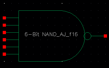
sequence has 6 bits I had to design a 6-bit NAND gate. Below are images of
the 6-bit NAND gate schematic, symbol and layout.

6-bit NAND Gate schematic

6-bit NAND gate symbol

6-bit NAND gate layout
On the output of the detector
I had to place a buffer that would amplify the output signal. I
calculated the Buffer value to be 5 so each buffer has a multiplier of 5
from the previous. This value was selected so that there wouldn't be
too much delay in the output of the detector circuit. Below are images
of the buffer schematic, symbol, and layout.

Buffer schematic

Buffer symbol

Buffer layout
The
detector circuit is made up of 6 DFF and the 6-bit NAND where the
outputs of the DFF all go into th NAND gate. Below are images of the
detector circuit, symbol, layout, DRC and LVS.

detector schematic

detector symbol

detector layout

detector DRC

detector LVS
The
simulation of the detector circuit should output a 1 when the signal
101011 appears. If any other signal appears the output should be 0.
Below are images of the simulation results of the detector.

detector simulation circuit

detector results for 101011
Zipfile for lab project placed here.
Return to EE421L Labs


