Lab 7 - ECE 421L 

Authored by Antanasia Jones

jonesa20@unlv.nevada.edu


11/16/16  


For this lab the goal was to design the basic building blocks of an Arithmetic Logic Unit (ALU) which are 8-bit inverter, NAND, NOR, AND  and OR along with an 8-bit 2-to-1 MUX/DEMUX and an 8-bit full adder. Note: All MOSFETs used in this lab are 6u/0.6u. 


In the first part of the lab I designed 8-bit inverter, NAND, AND, NOR, and OR gates. The inverter and NAND gate were used from previous labs and the NOR gate was implemented using schematic from Fig. 12.1 in the CMOS textbook. The OR and AND gates were implemented by placing an inverter on the output of the NOR and NAND gates. 

Using the example provided in lab 7 for the 4-bit inverter, the same idea was applied to making the 8-bit inverter and other logic gates. A symbol was created for each and a simulation was done in the same fashion as the 4-bit inverter. Shown below are the 8-bit logic gates, their symbols, and the simulation results (to save room only the simulation schematic of the 8-bit inverter is shown below; the schematics look similar for the other gates just with the inverter replaced with the corresponding gate). Along with the simulation results is a truth table to show the desired results. To save room the 


inv8.jpginv8_sym.jpg

                                       8-bit inverter schematic                                                                      8-bit inverter symbol

sim_inv8.jpg  

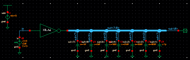
                             8-bit inverter simulation schematic

AAi
01
10
Inverter Truth Table
 

inv8_sim.jpg

                                                                   8-bit inverter simulation results 


nand8_sch.jpgnand8_sym.jpg

                                              8-bit NAND schematic                                                                      8-bit NAND symbol

ABAnandB
001
011
101
110

 NAND Truth Table 


nand8_sim.jpg

                                                                        8-bit NAND simulation results


nor8.jpgnor8_sym.jpg

                                                   8-bit NOR schematic                                                                      8-bit NOR symbol

ABAnorB
001
010
100
110

NOR Truth Table

nor8_sim.jpg

                                                                                            8-bit NOR simulation results 

and8.jpgand8_sym.jpg

                                         8-bit AND schematic                                                                      8-bit AND symbol

ABAandB
000
010
100
111

AND Truth Table

and8_sim.jpg

                                                                                      8-bit AND simulation results


or8.jpgor8_sym.jpg

                                                        8-bit OR schematic                                                                      8-bit OR symbol  

ABAorB
000
011
101
111

OR Truth Table

or8_sim.jpg

                                                                                     8-bit OR simulation results

For the next part of the lab I designed a 2-to-1 MUX/DEMUX. The MUX works as a selector to choose one input or another depending on the value of S. The circuit (shown below) can also work as DEMUX by simply making the output the input and the inputs the outputs. That way the value of S determines to which output the input will go to. Once this was designed a symbol was made for it a simulation was done to check its performance. Below are the images of the MUX/DEMUX, its symbol and the simulation results with a truth table. 


2-to-1_mux.jpg  2-to-1_mux_sym.jpg

                                  MUX/DEMUX schematic                                      MUX/DEMUX symbol

ABSZ
0000
0010
0101
0110
1000
1011
1101
1111

MUX/DEMUX Truth Table


 2-to-1_mux_sim.jpg

                                                             MUX/DEMUX simulation results


The 8-bit MUX/DEMUX was designed similar to the gates. However, the Si input was removed and was replace with an inverter on the S input. Below are images of the 8-bit MUX/DEMUX schematic, the represented symbol and the simulation schematic and results. 


2-to-1_mux8_sch.jpg 2-to-1_mux8_sym.jpg

                          8-bit MUX/DEMUX schematic                                                                      8-bit MUX/DEMUX symbol


sim_2-to-1_mux8.jpg

                                        8-bit MUX/DEMUX simulation schematic 

2-to-1_mux8_sim.jpg

                                                              8-bit MUX/DEMUX simulation results


For the final part of the lab I had to draft a full-adder from Fig. 12.20 of the CMOS textbook. The drafted schematic, full adder symbol, simulation results and a truth table for the full adder are shown below. 


full_adder_sch.jpg  sim_full_adder_sch.jpg  

                                                 full-adder schematic                                                               full-adder simulation schematic with symbol


ABCSC+1
00000
00110
01010
01101
10010
10101
11001
11111

full-adder Truth Table


 sim_full_adder.jpg

                                                                     Full-adder simulation results


The 8-bit full adder was drafted along with the symbol. For the full adder to work the carry out of one adder has to connect to the carry in of the next full adder, so the looping on the carry in in made in the 8-bit full adder schematic. So for the symbol there is only one carry in input. The schematic, symbol and simulation results are shown below. 


8_bit_fa_sch.jpg 8_bit_fa_sym.jpg

                                   8-bit full-adder schematic                                                                      8-bit full-adder symbol


 sim_fa_sch.jpg

                        8-bit full adder simulation schematic


 8_bit_fa_sim.jpg

                                                      8-bit full adder simulation results


A layout was done of the 8-bit full adder and an DRC and LVS were performed on the layout. Below are images of a single full adder layout, the 8-bit full adder layout and the LVS and DRC for the 8-bit full adder layout. 


fa_layout.jpg

                                              1-bit full-adder layout

     8_bit_fa_layout.jpg

                                                                                                                   8-bit full-adder layout


8_bit_fa_drc.jpg  fa_lvs.jpg

                                         8-bit full-adder DRC                                                                                    8-bit full-adder LVS


A zipfile of all the cells used in this lab is placed here 


Return to EE421L Labs