Lab 5 - ECE 421L
Authored
by Antanasia Jones
jonesa20@unlv.nevada.edu
10/5/16
For this lab I had to create schematics and layouts for a CMOS inverter using NMOS and PMOS inverters.
In
the first part of the lab I designed a schematic for a CMOS inverter
using a 12u/0.6u (=W/L) PMOS and a 6u/0.6u NMOS where the PMOS is
connected to Vdd and the NMOS is connected to ground and the gates of
both devices are connected to each other. The input being A and output
being Ai. Then I created a symbol for the schematic where the input is
A and the output is Ai. The images below shows the 12u/6u inverter and
the symbol representing the inverter.


CMOS schematic 12u/6u
CMOS symbol 12u/6u
I
then had to design a similar schematic where the PMOS and NMOS were 4
times larger. This is done by using the multiplier in the PMOS/NMOS
component properties and set M=4. Then I created a symbol for the
schematic. The images below shows the 48u/24u inverter and the symbol
representing the inverter.


CMOS schematic 48u/24u
CMOS symbol 48u/24u
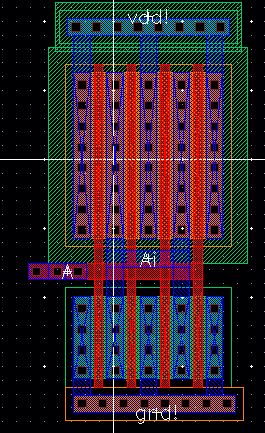
For the next part
of the lab I created a layout for the two CMOS inverters. Each layout
having pins on the metal 1 layer of A, Ai, vdd! and gnd!, where vdd!
and gnd! represent universal vdd and universal gnd. Below are images of
the layouts and extracted views of each CMOS inverter.
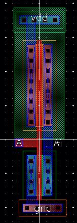


12u/6u inverter layout and extracted
view
48u/24u
inverter layout and extracted view
I then performed
DRC test on both inverter layouts to make sure all the rules were
followed. And then I performed LVS on the schematics and the extracted
views of each inverter. The images below show the DRC and LVS tests for
the 12u/6u and the 48u/24u inverters


12u/6u inverter DRC test
12u/6u inverter LVS test


48u/12u inverter DRC test
48u/24u inverter LVS
test
In
the final part of the lab I created a simulation circuit of both the
12u/6u inverter and the 48u/24u inverter driving a capacitive load
having vlaues of 100fF, 1pF, 10pF and 100pF. Each capacitive load was
simulated using the normal simulation tool and the Ultra-Sim tool,
which is meant to provide a more accurate transient response. Below are
the images of the schematics and the simulations of each capacitive
load using the normal simulation tool and the Ultra-Sim tool. for each
schematic.

12u/6u inverter simulation
circuit


100fF
100f ultra-sim


1pF
1pF ultra-sim


10pF
10pF ultra-sim


100pF
100pF ultra-sim

48u/24u inverter simulation
circuit


100fF
100fF ultra-sim


1pF
1pF ultra-sim


10pF
10pF ultra-sim


100pF
100pF ultra-sim
It
should be noted that as the capacitor size increases the more
attentuated the output signal becomes. This happens because with a
larger capacitor the longer it takes to charge and discharge. So with a
small capacitor, such as 100fF, the capacitor charges rather
quickly on the falling edge of the input and discharges quickly on the
rising edge. Where as with a later capacitor, such as 100pF, the
capacitor takes more time to charge on the falling edge and to
discharge on the rising edge. Also for this capacitve load it should be
noted that unlike the capacitve loads it never completely discharges or
charges due to there not being enough time between pulses to allow
the capacitor to fully charge or discharge.
The zipfile containing all these cells are places here.
Return to EE 421L Labs