Lab 2 - ECE 421L 

Authored by Antanasia Jones

jonesa20@unlv.nevada.edu

9/10/2016


In this lab we had to design and implement our own 10-bit Digital-to-Analog (DAC) converter and compare its function to an ideal DAC.


Return to EE 421L Labs


Prelab  

For the Prelab we had to upload a file, lab2.zip, into the CMOSedu directory, unzip the file and place the code DEFINE lab2 $HOME/CMOSedu/labs on the bottom of the cds.lib file. 


cdslib.jpg

Once this was completed, open up Cadence, find the lab2 library and open sim_Ideal_ADC_DAC schematic. Run a transient simulation and plot Vin and Vout.


ideal_adc_dac_sim.jpg


From the simulation above, it should be noted that Vout (blue) has a similar waveform to Vin (red) however the signal is not as smooth as the original. This is due to the signal maintaining some of the characteristics that it had when it was converted to a digital signal by the ADC. The use of a low-pass filter, or RC circuit, could be used to help smooth out the signal.


An analog-to-digital works by receiving an analog signal and manipulating it by converting the output of that signal into digital impulses or bits. a digital-to-analog converters works similarly but in reverse by taking a digital signal given in bits and converting it into an analog signal. To demonstrate my understanding of the ADC and DAC, I simulated the circuit, changing Vin to have a 3V amplitude and a 3V offset, making the signal 6V peak-to-peak.
 
Sim_clamp.jpg

The simulation above shows that Vout gets clamped off at 5V. This happens because the DAC is being feed a Vdd of 5V which places a limit on the output voltage. Since the output is limtied to 5V the signal clamps off at 5V regardless of the value of Vin.


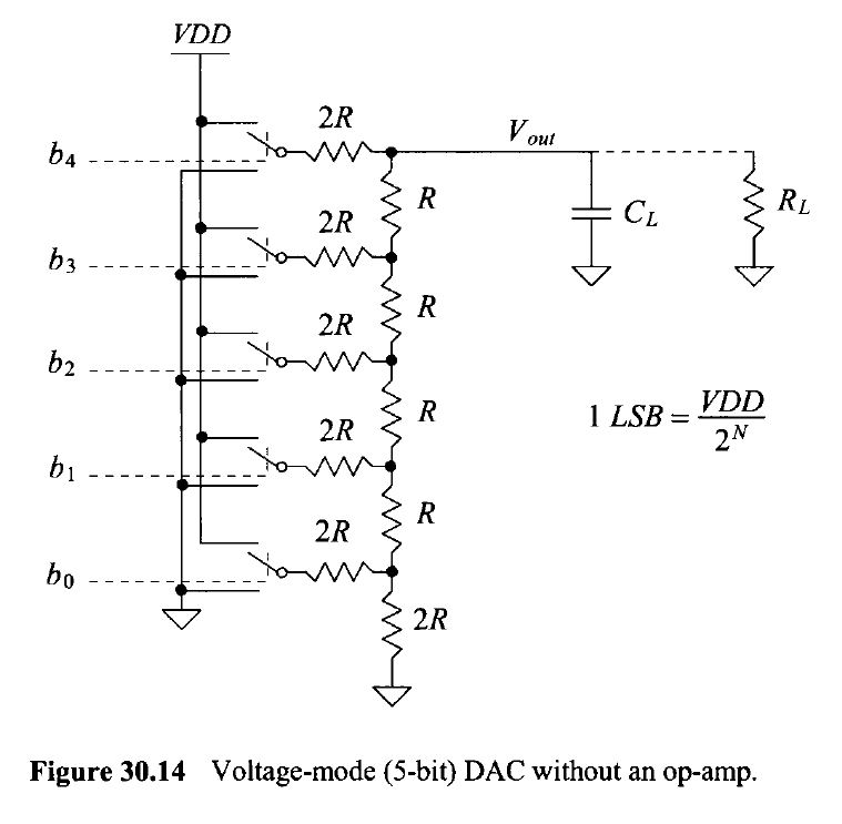
To the find the least significant bit (LSB) use the equation Vdd/2^N, where N is the number of bits in the DAC, in this case being 10. 

So, the value of LSB = 5V/2^10 = 5V/1024= 0.00488V or 4.88mV. For the ideal DAC used here, the LSB is located at B0. 


Sim_LSB.jpg

The simulation shows the LSB (pink) and how it changes at relatively steady, or every 4.88mV, and these impulses line up with the jagged edges of the output signal. 


Lab 

The design of the 10-bit DAC involved combining multiple 10k resistors, similar to the topology seen in Fig 30.14  however instead of there being 5 bits there had to be 10 bits. the design also did not need a Vdd or any load resistors or capacitors. Once the schematic was completed I created a symbol of for the DAC using the symbol for the Ideal DAC given and modifying it by removing the Vrefp and Vrefm and Vdd. 

  
                                                                               MyDAC_layout.jpg   MyDAC_Symbol.jpg


To find the output resistance value of the 10-bit DAC that was designed just simply simplify the circuit by combining the resistors in series and in parallel as shown below. 


                                                                    output_resistor_value.jpg


To determine the time delay of the 10-bit DAC that was designed I simulated the circuit shown below, where B9 is connected to 5V pulse input, the pins are grounded and the DAC is driving a 10pF load. 


 Sim_pulse.jpg

The time delay td, the time it takes for the output to reach 50%, can be estimated by using 0.7RC, where R=10K and C=10pF. In this case td=700ns. The max output voltage is approximately 2.5V so the time delay should occur when Vout reaches about 1.25V which occurs at about 700ns as shown in by the circle in the image above. 


Replacing the ideal DAC with My DAC in the circuit and simulating it to ensure that it works properly.

My_DAC_sim.jpg

 From the simulation it can be seen that DAC works similar to that of the ideal DAC. The simulation results are not exactly the same however there is little deviation from the ideal DAC. 
 
When My DAC drives a 10pF load we end up with the following simulation which has a similar result to an RC series circuit.

 Sim_10pF.jpg


With the DAC driving a 10k load and a 10pF load in parallel we get the following simulation. The simulation is much smoother than the original and the drop in amplitude has to do with the 10k resistor causing a voltage drop at Vout.
 
Sim_RC_parallel.jpg
   
With a 10k resistor load the output voltage Vout can be determined by using a voltage divider since the output resistance of the DAC is also 10k. So Vout= Vin [10k/( 10k+10k)] = Vin (1/2) = 2.5V. This result can be seen in the simulation below.

 Sim_10K_load.jpg

If the switches in a real circuit were to have a very large resistance compared to R, then the 2R will combine in series with the switch resistance. So when the output voltage of the circuit is calculated the starting from the bottom it will be 2R\\(2R+ switch resistance) = [2R*2R*switch resistance]/[2R+2R+switch resistance] = [4R^2*switch resistance]/[4R+switch resistance]. When fully calculated the output resistance will end up being less than R.