Lab
Project
Design
a circuit that takes a serial input and detects
the sequence 101011
Download
project library (labProj.zip) here
Authored
by Tyler Huddleston, huddle10@unlv.nevada.edu
11/30/2016
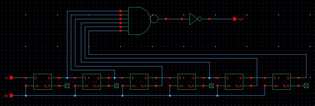
Part 1: 101011 Sequence Detector
schematic and simulations
| Schematic |
|
|
|
Topology:
- The sequence
detector has 3 pins:
- in (input) -
sequential logic signal input into detector
- clk (input) -
clock signal
- out (output) -
logic value that outputs HIGH if the sequence has been detected and LOW
otherwise
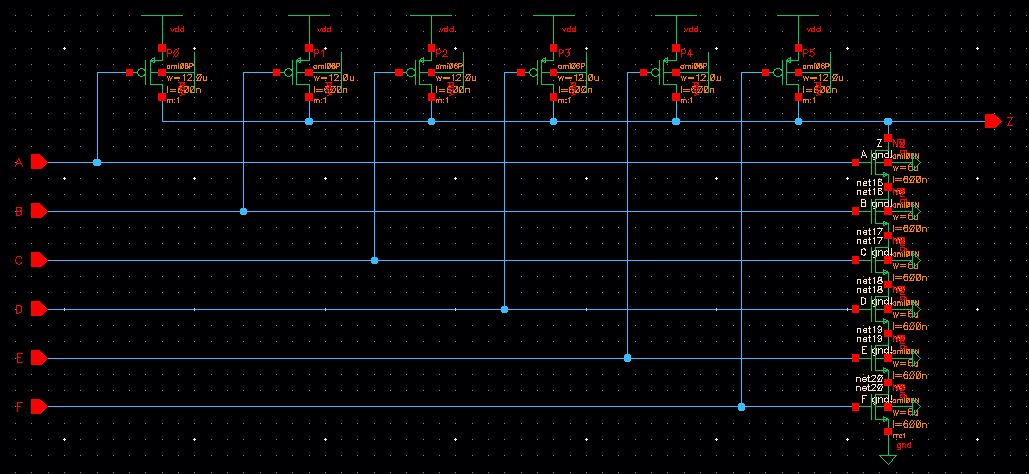
- It consists of
6 D flip-flops, a 6-input NAND gate, and an inverter:
- D flip-flops:
store and output a bit for one clock cycle
- output Q or
Q_N to NAND gate depending on which bit is required at the D flip-flop
to
detect the sequence
- 6-input NAND
gate outputs LOW if the Q or Q_N values at its inputs are all HIGH, and
out goes HIGH after inverter
- NAND gate and
inverter were chosen over an AND gate, because the AND gate is a NAND
gate with an inverter and if the AND were to be used in a NAND
operation another inverter would have to be added to it - that is, to
achieve an AND operation with a NAND and inverter requires less
components than achieving a NAND operation with an AND and an inverter
|
Operation:
- Sequential
input into 'in' is propagated through the D flip-flops
- To detect
101011, the D flip-flops are arranged in reverse order, such that the
least significant bit of the sequence is at the end of the register -
that is, the least significant bit is detected by the right-most D
flip-flop
- If the D
flip-flop of the register is to detect a 1 in the sequence, its Q
output is sent to the NAND gate
- If the D
flip-flop of the register is to detect a 0 in the sequence, its Q_N
output is sent to the NAND gate
- The NAND and
inverter operate as an AND gate, such that when all of its inputs are
HIGH, the output, 'out', is HIGH, indicating that the sequence has been
detected
|
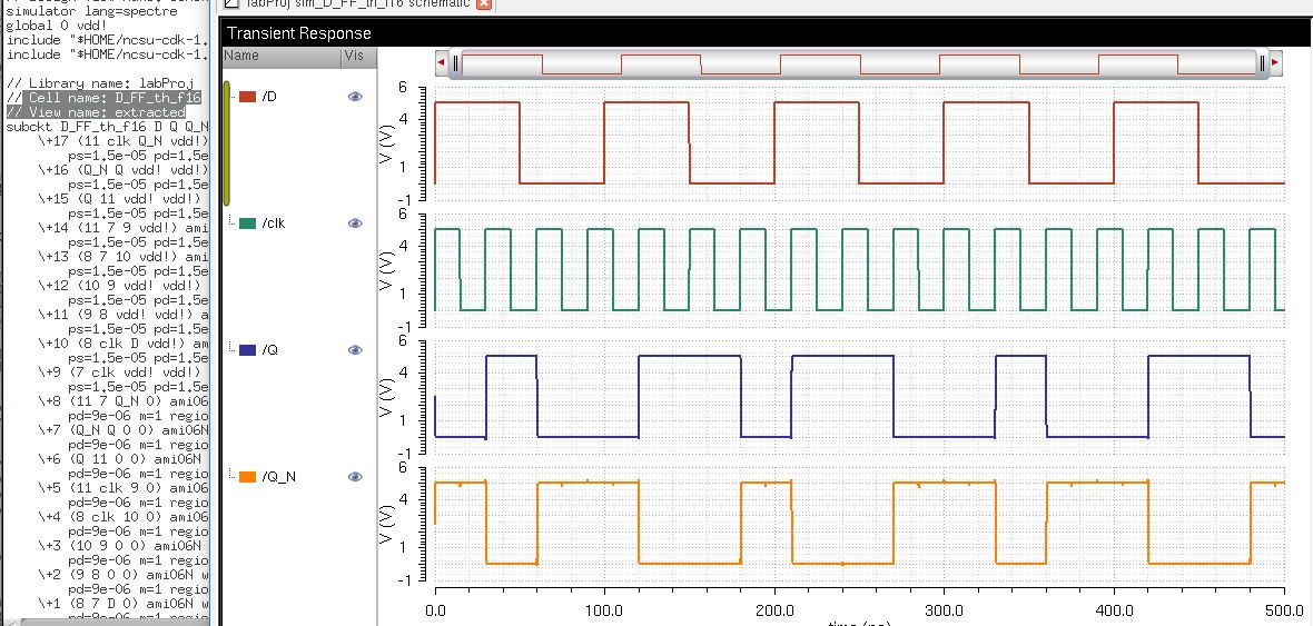
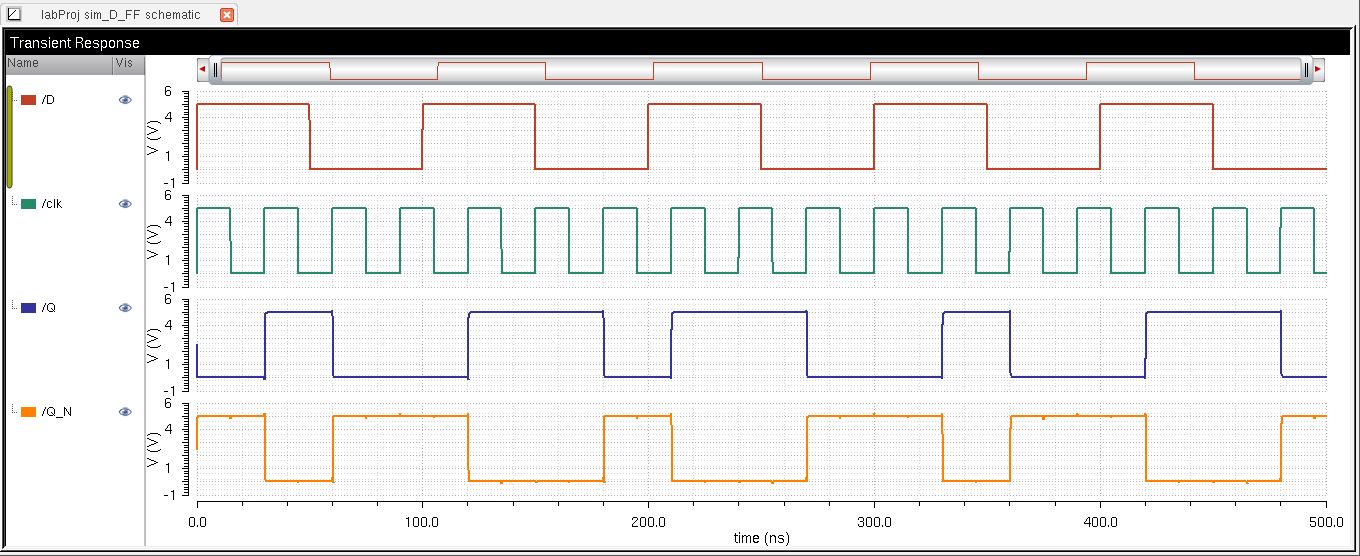
Simulation
|
Simulation
Schematic
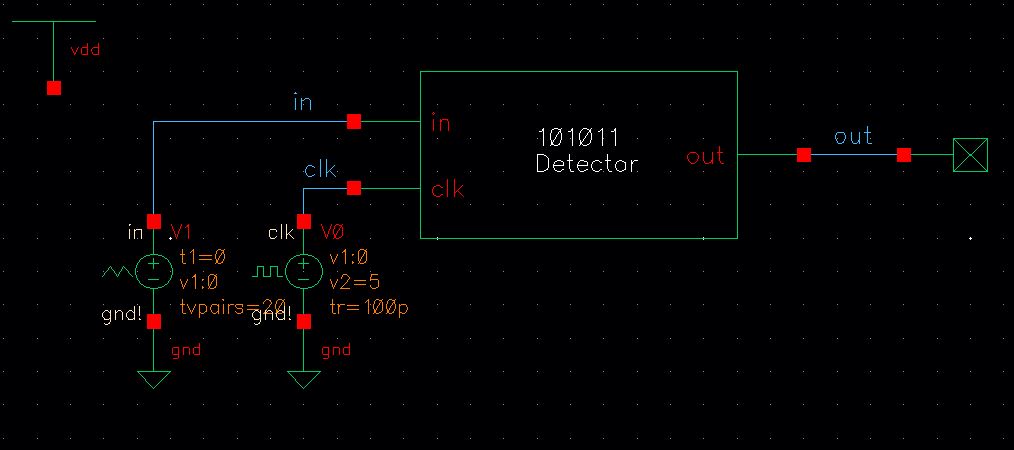
- A piecewise
function of various logic levels and a 50ns period clock signal are
input to the detector circuit
|
|
Simulation
Results
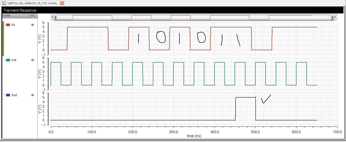
- Operation of
the detector works as expected:
- it is LOW when
101011 has not been input to the register
- it is HIGH
when 101011 has been input to the register
|
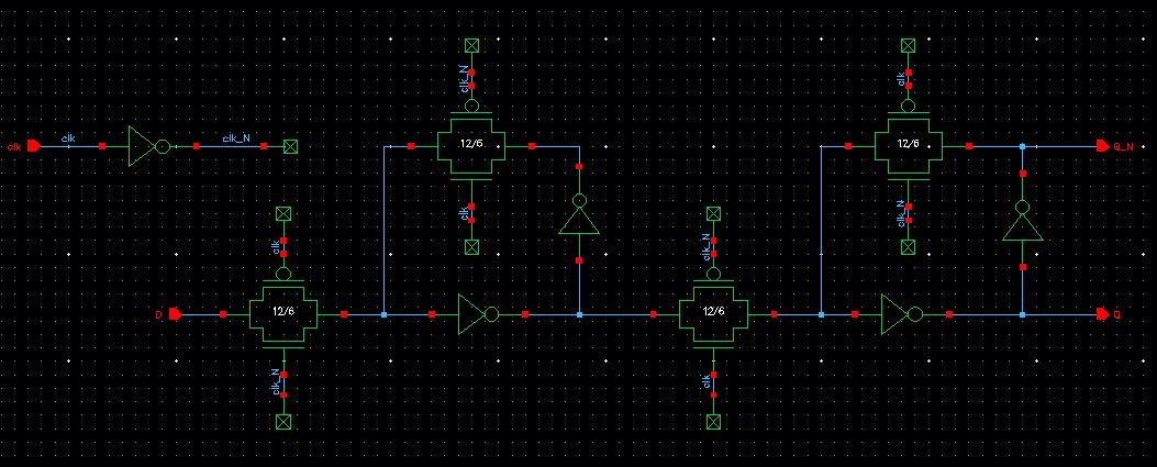
Sequence Detector Modules:
D
Flip-Flop
Schematic
 |
Simulation
schematic
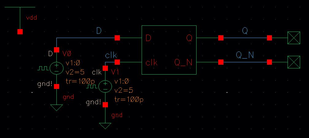 |
Simulation
results
 |
6
input NAND
Schematic
 |
Simulation
schematic
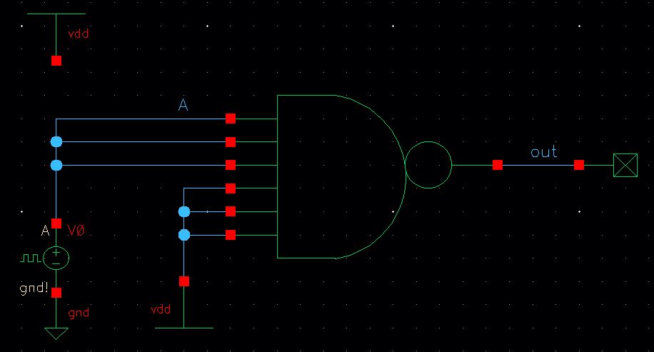 |
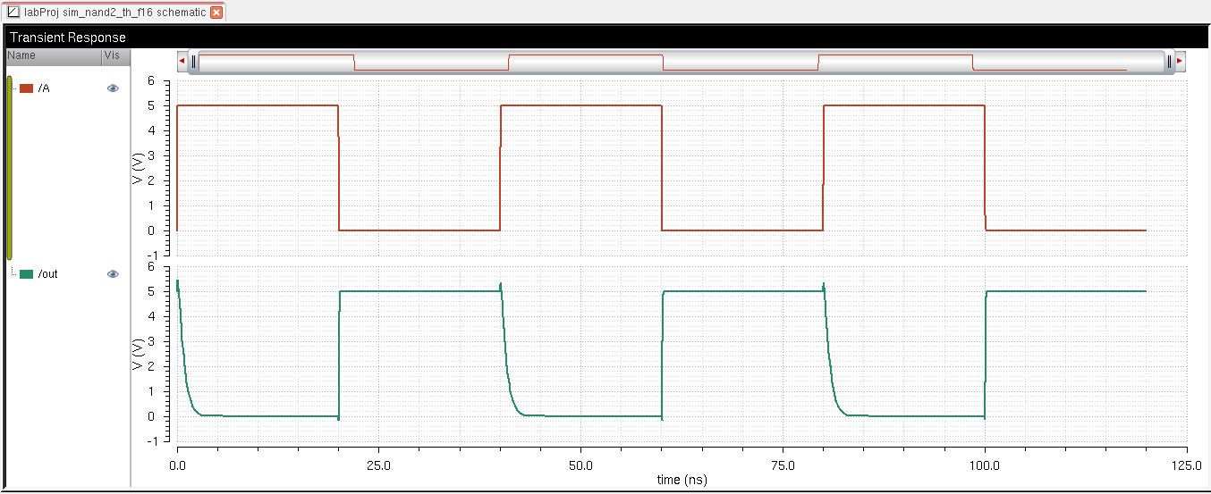
Simulation
results
 |
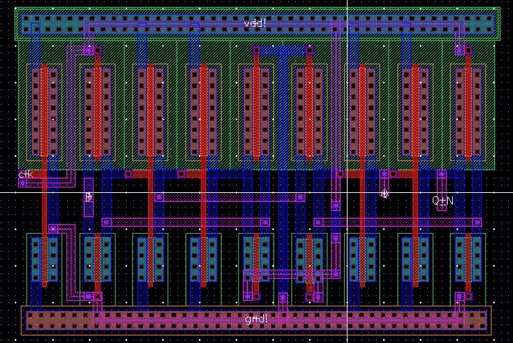
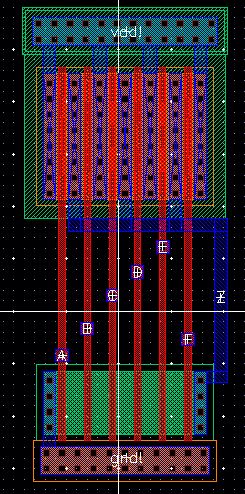
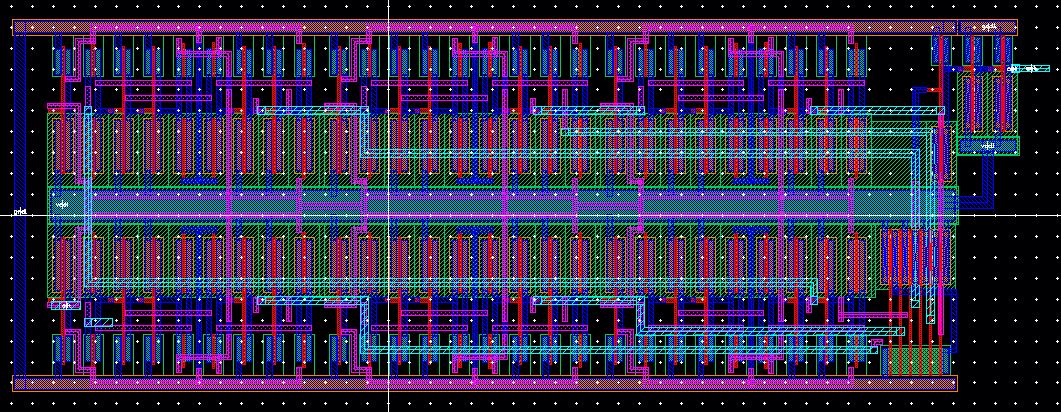
Part 2: layout detector circuit
Layout
of detector circuit:
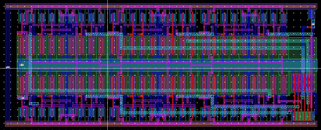
- 6 D flip-flops
are arranged in two rows for compact design
- one large
n-well fills the center of the layout with one large ntap vdd rail
shared by all of the PMOSs
- two large ptap
ground rails run along the top and bottom and are shared by the NMOSs
- each D
flip-flop is cascaded with its Q output connected to the D input of the
next D flip-flop
- the Q or Q_N
output connected to the 6-input NAND gate on the bottom right
- the NAND gate
is output to the inverter at the top right
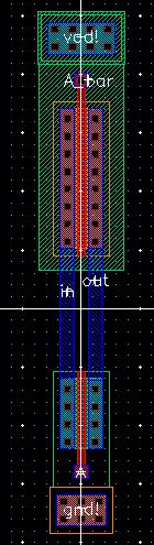
Close up of
first D flip-flop (most significant bit)
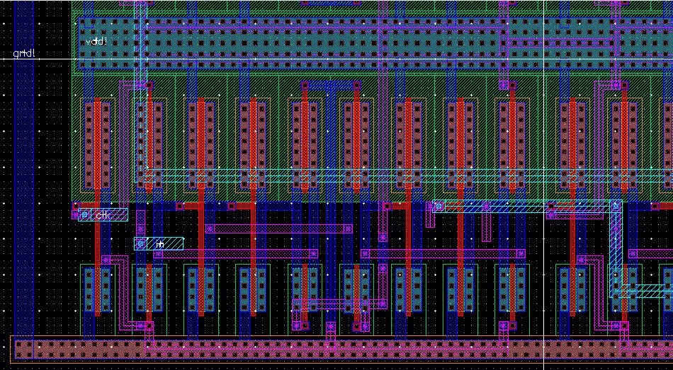 |
- in and clk are
connected on metal3
- vdd and ground
are connected on metal1
|
Close
up of NAND gate connectins and 3rd D flip-flop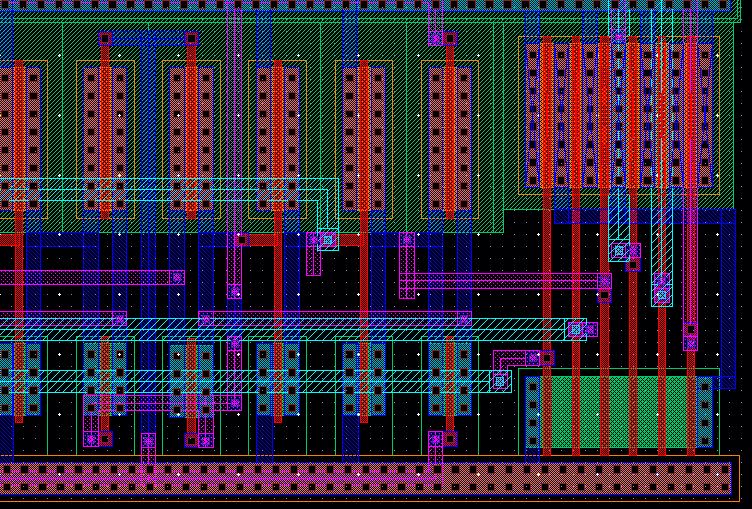 |
- the Q and Q_N
outputs of each D flip-flop connec to the input of the 6-input NAND gate
|
Close
up of inverter and 4th D flip-flop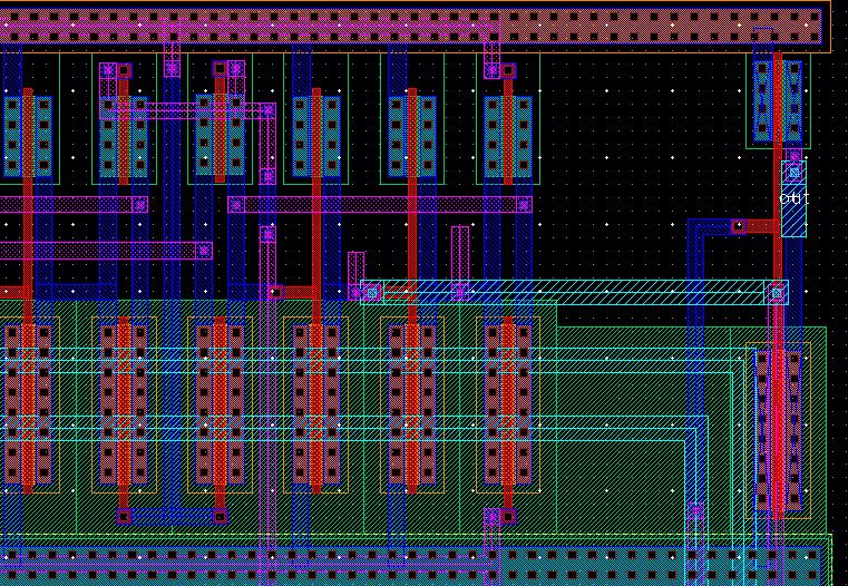 |
- the output
from the NAND gate is input to the inverter (metal1 route left of the
inverter) with the out pin on metal3
|
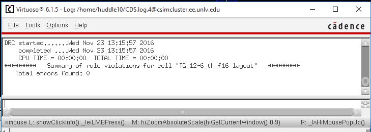
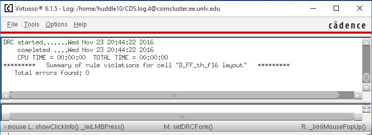
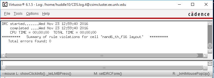
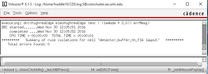
DRCs
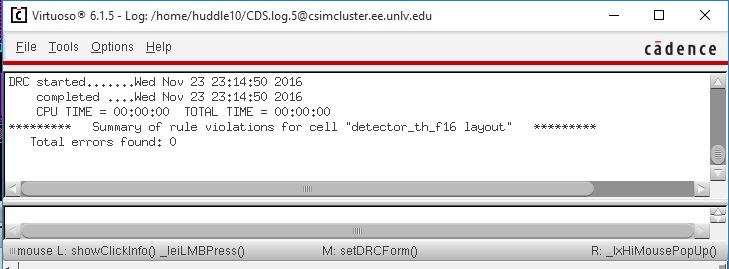 |
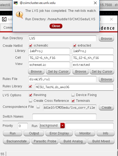
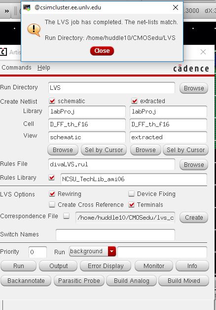
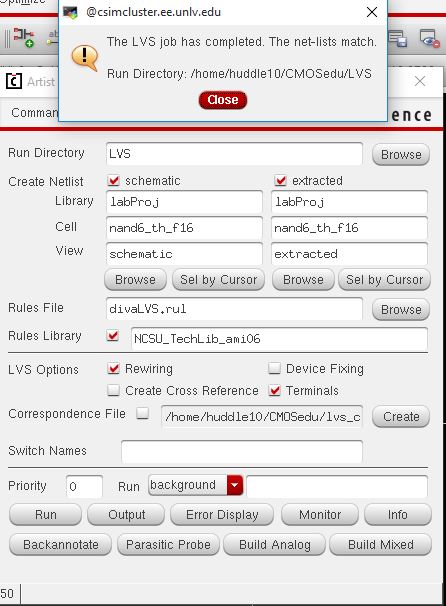
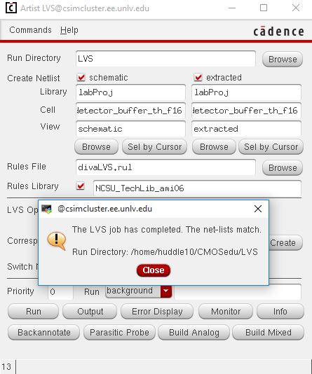
LVSs
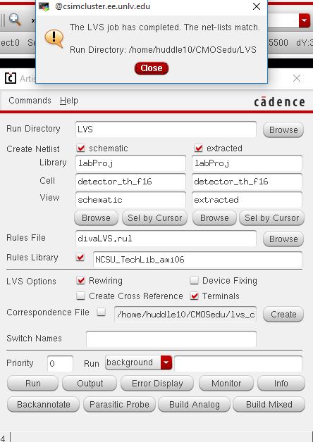 |
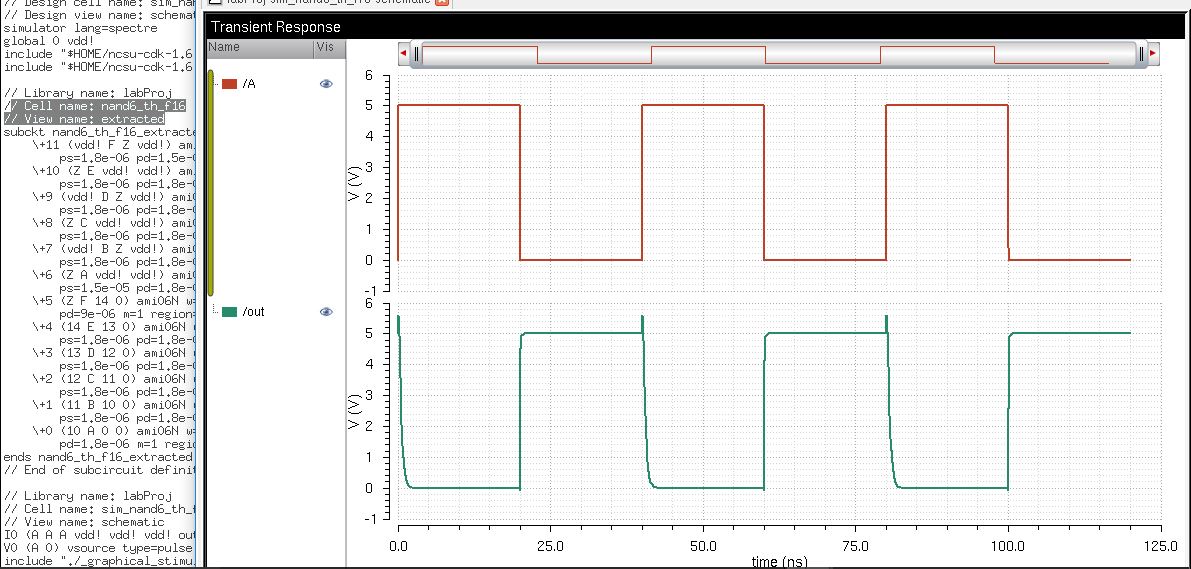
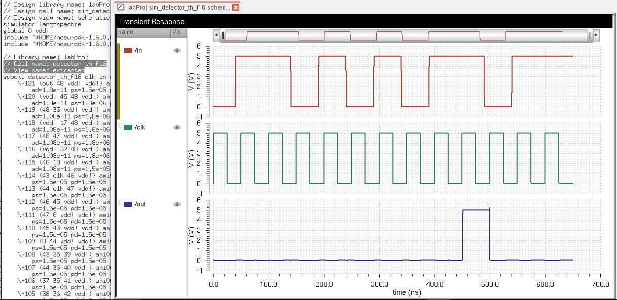
Verifying
the operation of extracted layout:
Extracted
layout simulation matches schematic simulation
Connecting
detector to buffer for chip layout
Schematic
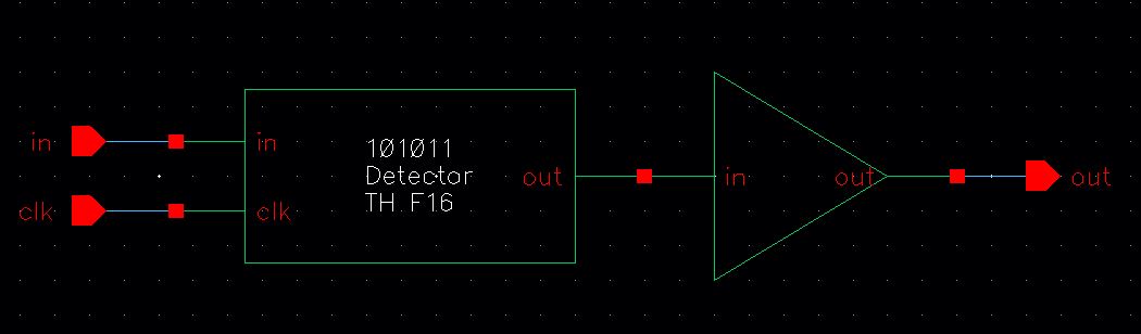 |
Layout
|
DRCs
 |
LVSs
 |
Return
to EE 421L Labs
Return
to my Labs Index