Lab 7 - ECE 421L
Using buses and arrays in the design of word inverters, muxes, and high-speed adders
Schematic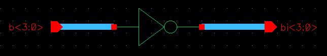 |
Simulation Schematic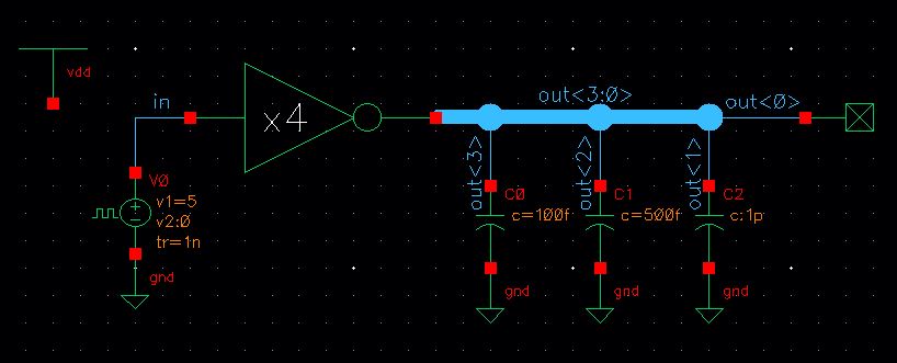 | Simulation Results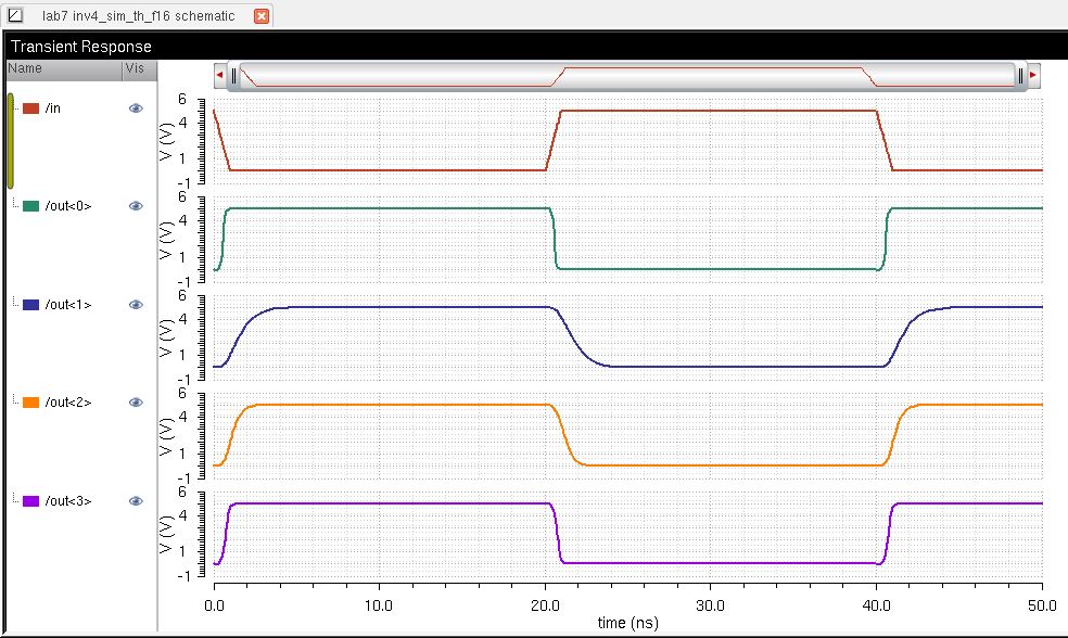 |
Schematic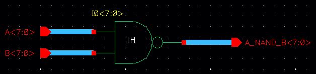 |
Simulation Schematic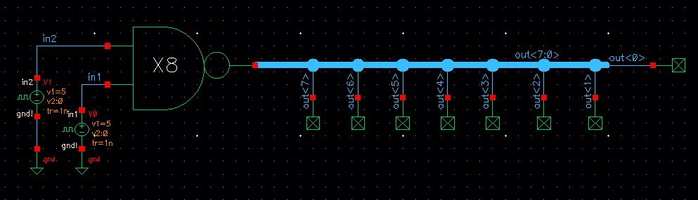 | Simulation Results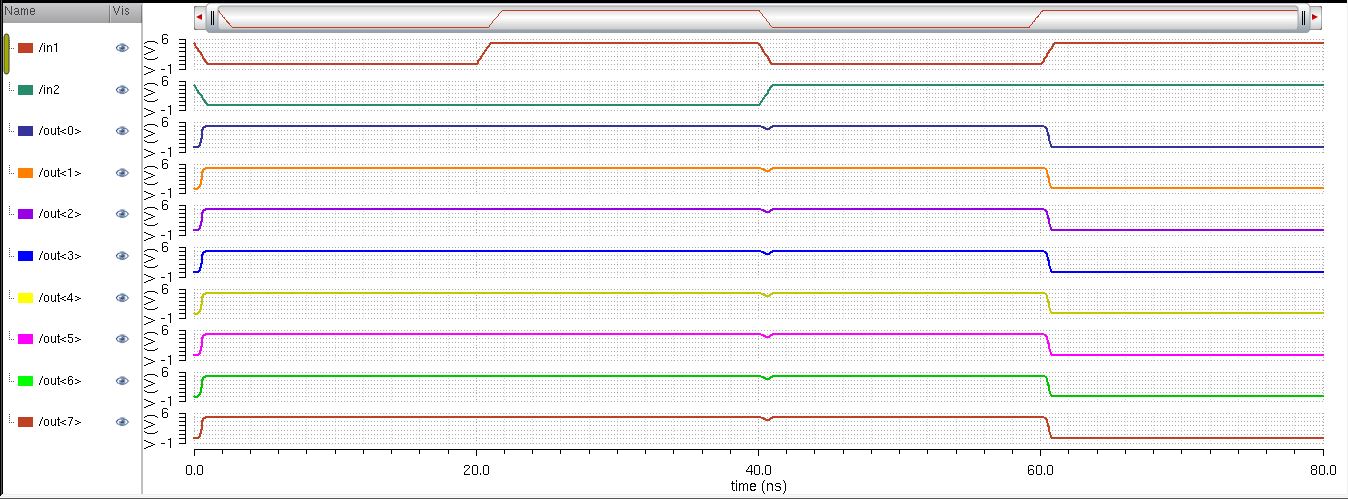 |
Schematic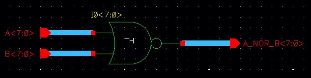 |
Simulation Schematic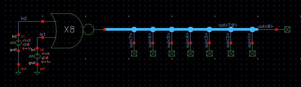 | Simulation Results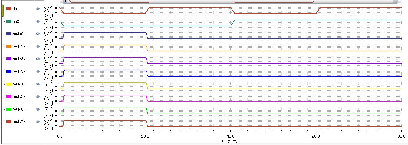 |
Schematic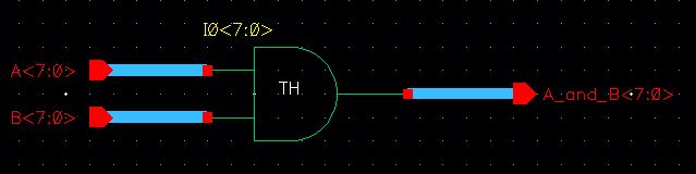 |
Simulation Schematic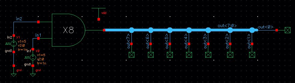 | Simulation Results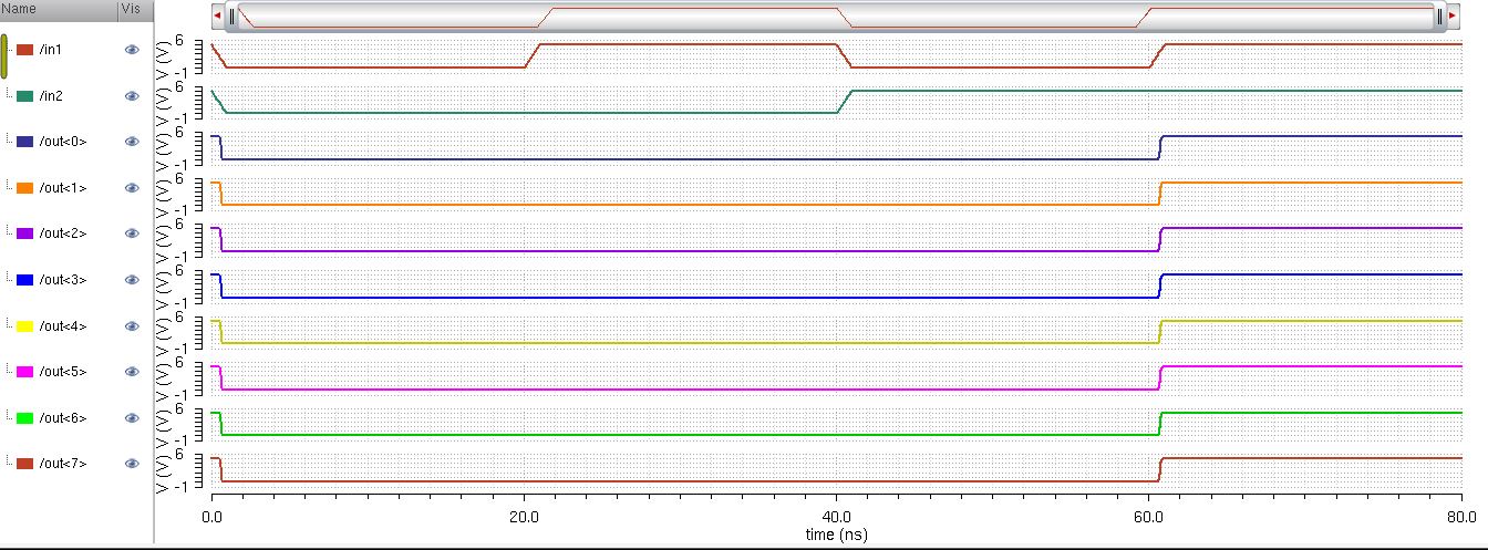 |
Schematic |
Simulation Schematic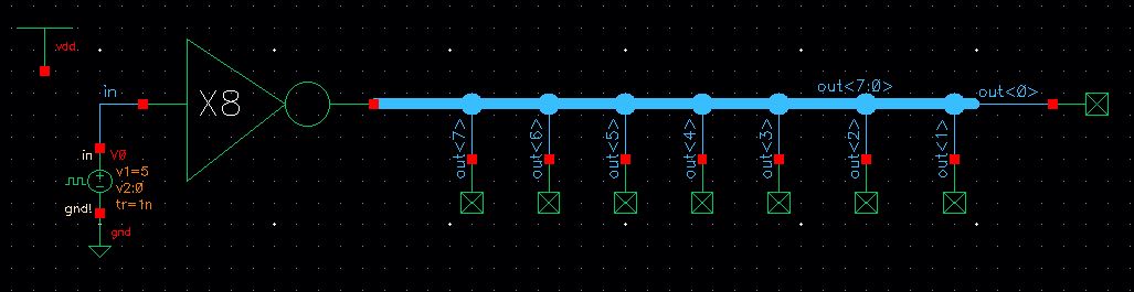 | Simulation Results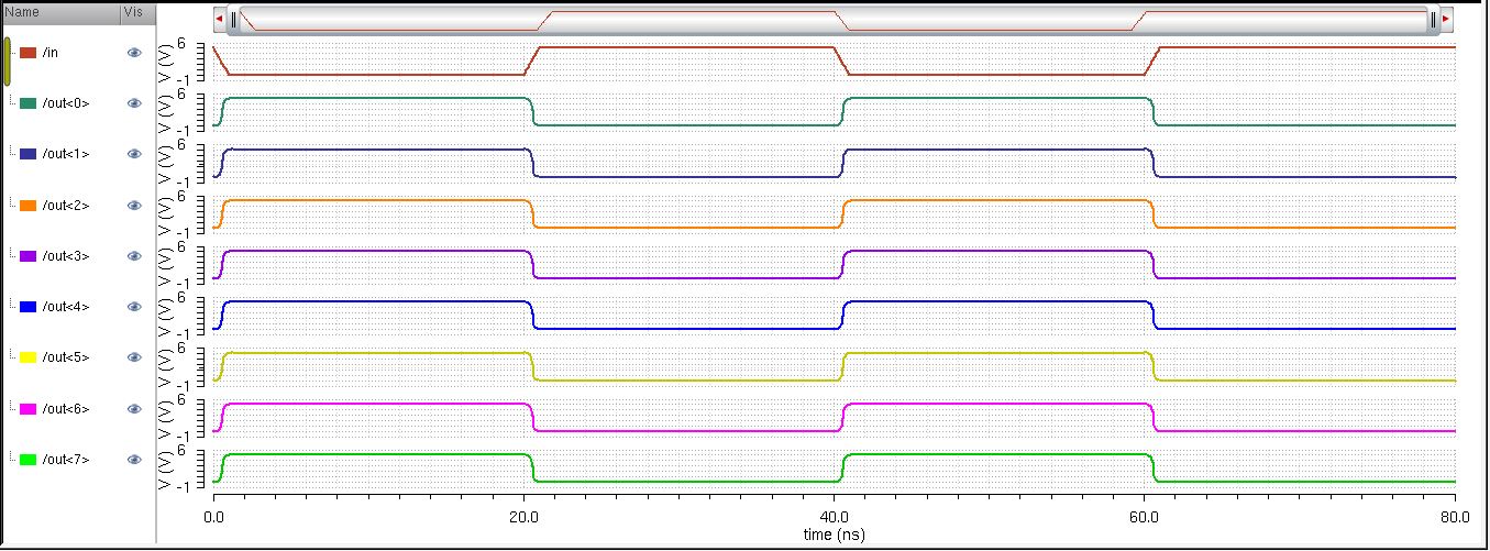 |
Schematic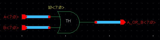 |
Simulation Schematic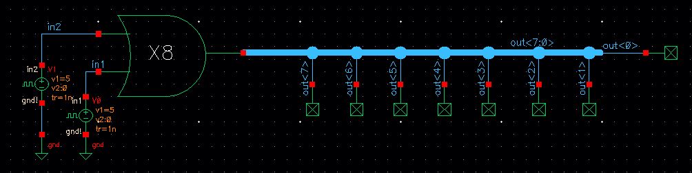 | Simulation Results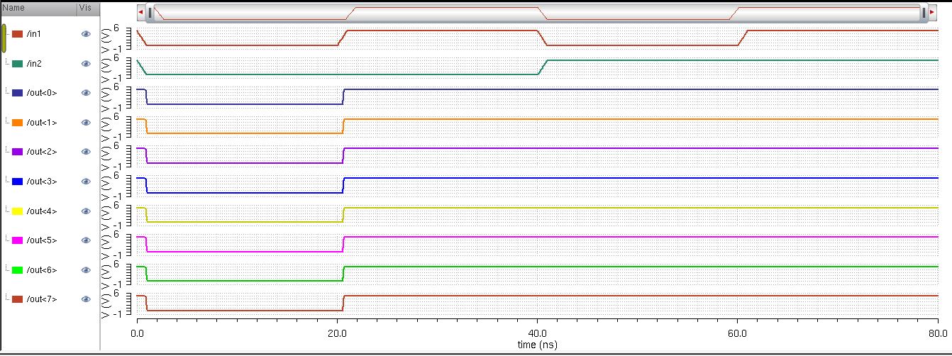 |
Schematic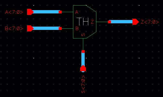 | Schematic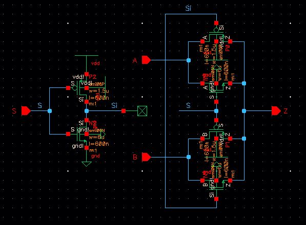 |
Simulation Schematic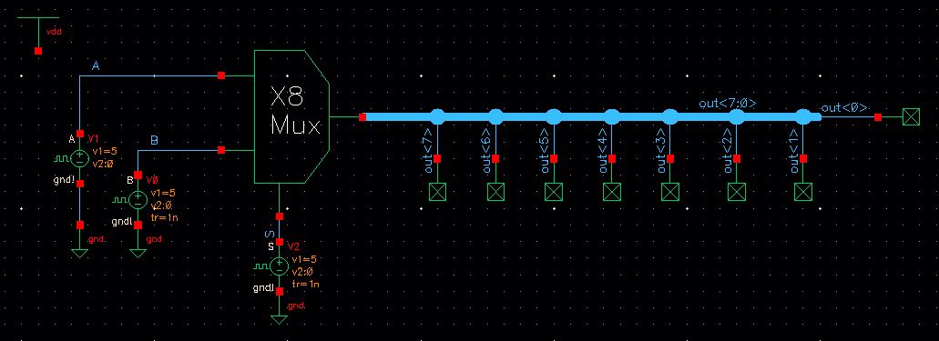 | Simulation Results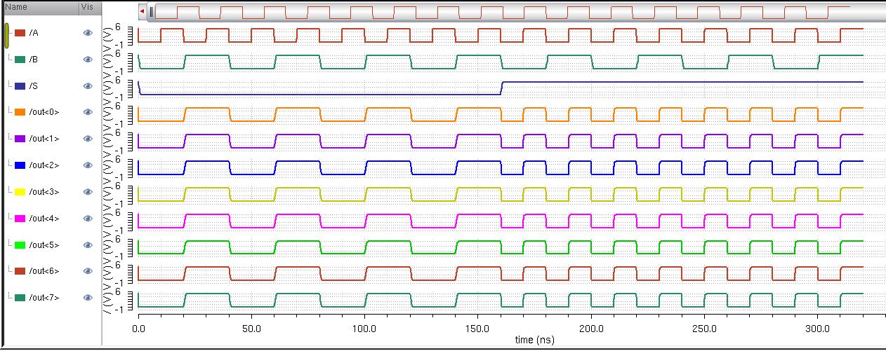 When S=0, the output is A. When S=1, the output is B. |
Schematic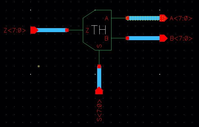 | Schematic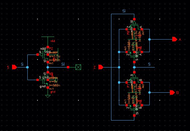 |
Simulation Schematic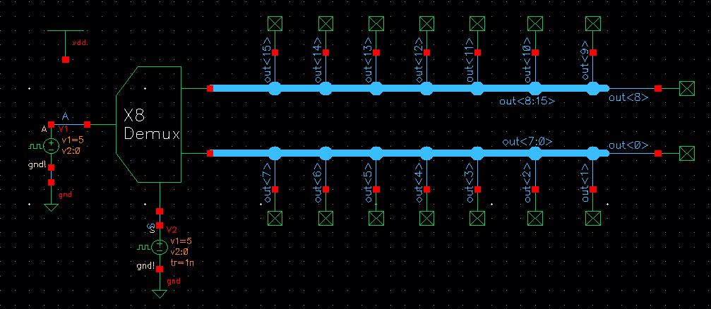 | Simulation Results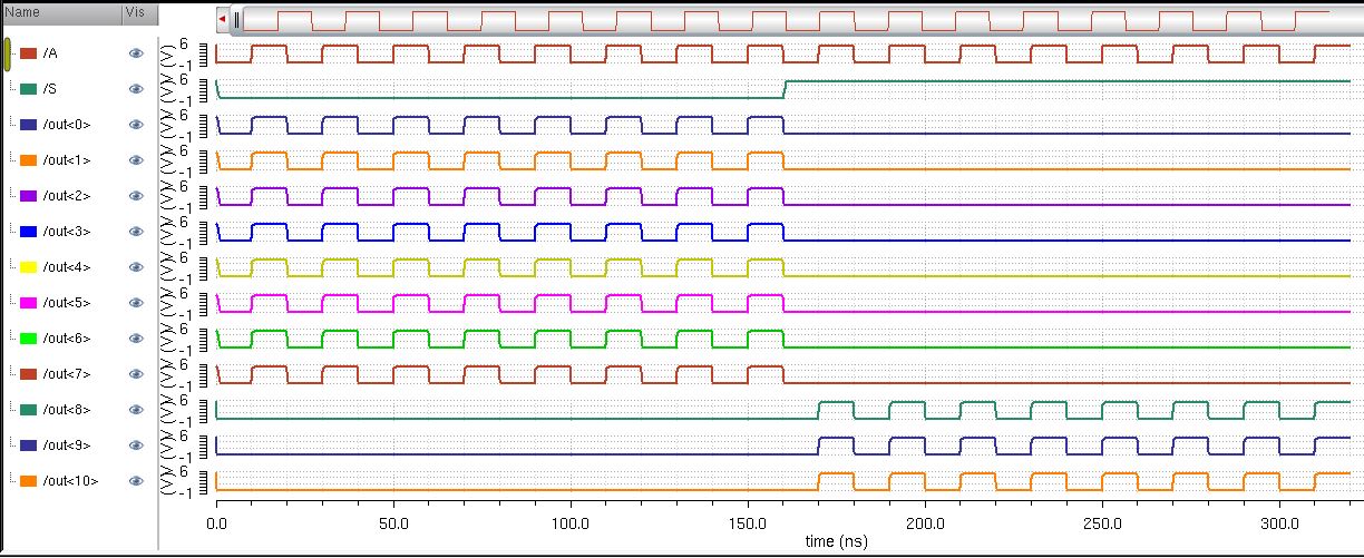 When S=0, the input is sent to A. When S=1, the input is sent to B. |
Schematic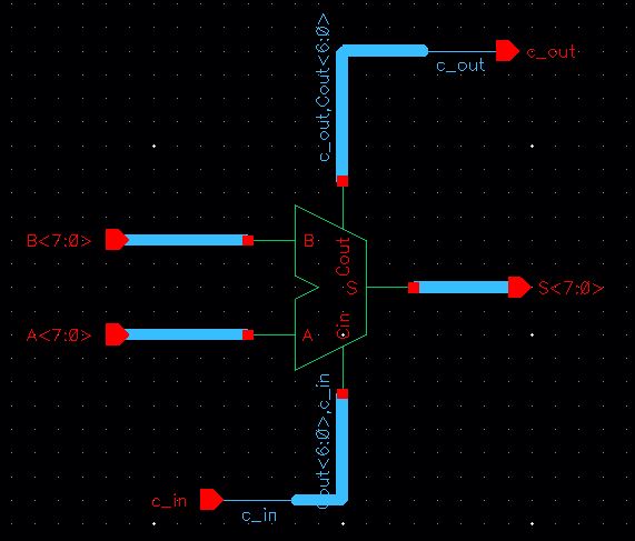 | Schematic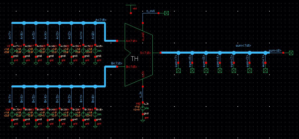 |
Layout  |
Layout Single Section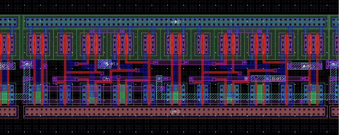 |
LVS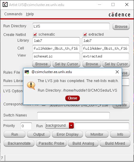 | DRC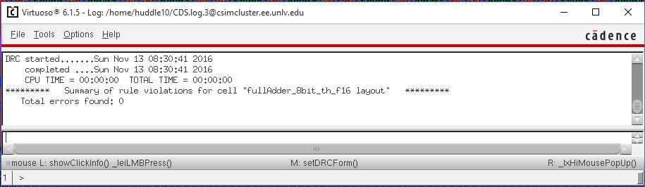 |
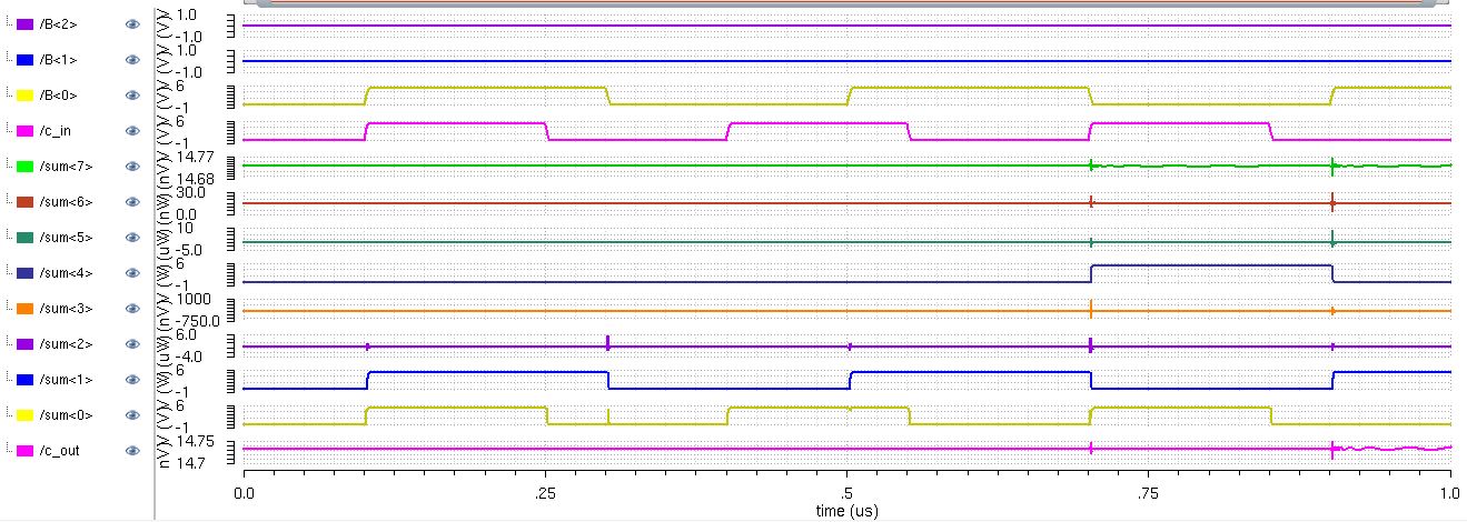
Simulation Results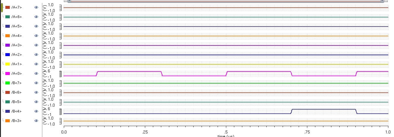 |
 |