Lab 4 -
ECE 421L
IV
characteristics and layout of NMOS and PMOS devices in ON's C5 process
Authored
by Tyler Huddleston, huddle10@unlv.nevada.edu
9/28/2016
This
lab consists of designing layouts, schematics, and symbols for NMOS and
PMOS transistors, as well as verifying they meet the design rules and
simulate to work as expected. It was completed by following
the
steps outlined in Tutorial 2.
Pre-lab Work
The pre-lab consisted of:
- Reading through the lab
- Backing up my work
- Completing Tutorial 2 - making note that the NMOS body is at ground
and PMOS body is at VDD
My projects are backed up to my hard-drive and Dropbox account (seen on
the left)
The NMOS and PMOS layouts and symbols were designed by following
Tutorial 2:
Lab Work
- Generate 4 schematics
and simulations
(see the examples in the Ch6_IC61 library, but note that for the PMOS
body should be at vdd! instead of gnd!):
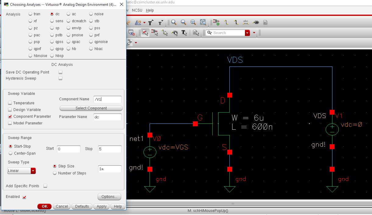
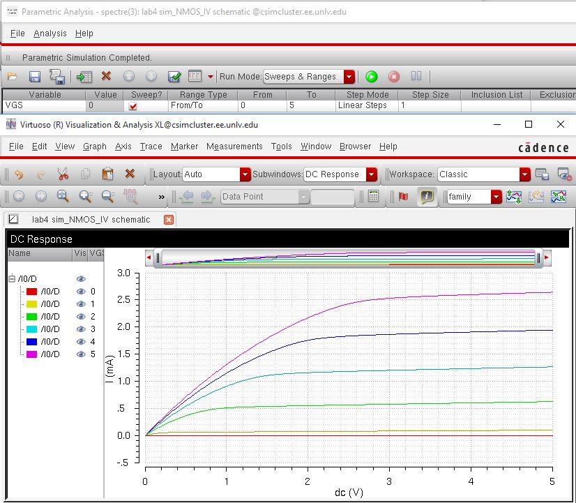
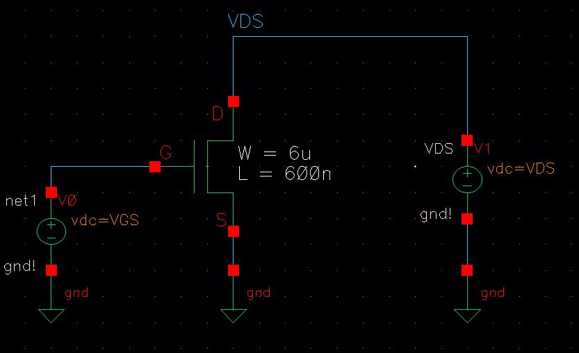
- A schematic for
simulating ID
v. VDS of an NMOS device for VGS varying from 0 to 5 V in 1 V steps
while VDS varies from 0 to 5 V in 1 mV steps. Use a 6u/600n
width-to-length ratio.
- The schematic and
simulation results using my NMOS device designed in Tutorial 2:
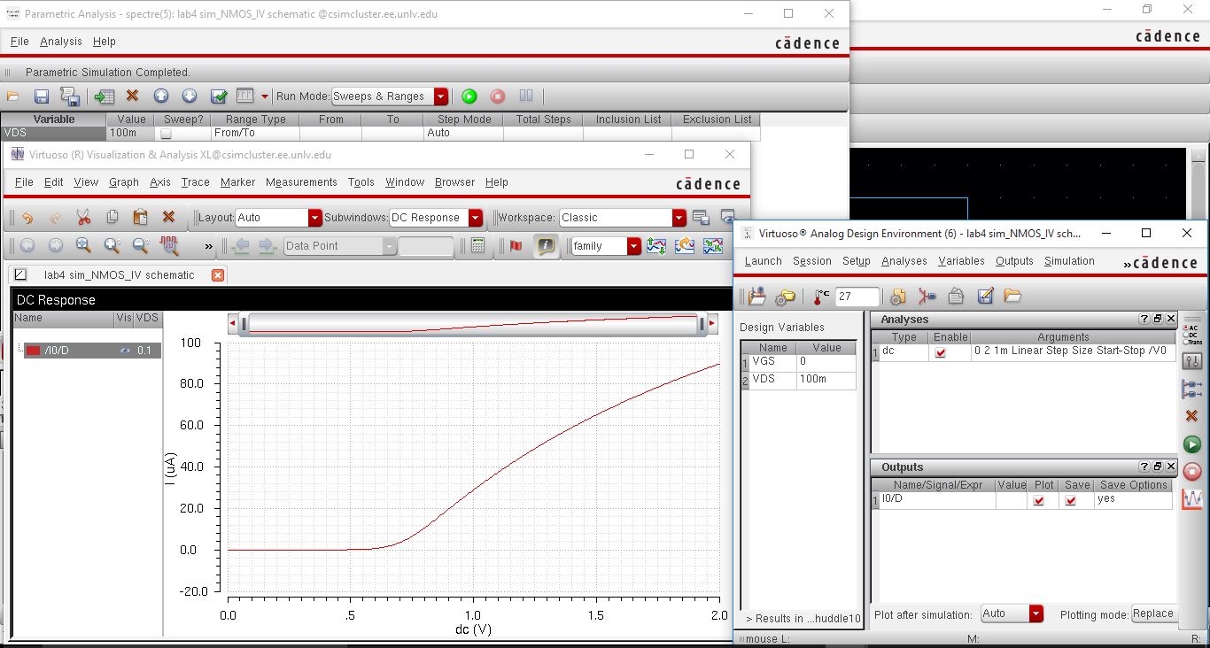
- A
schematic for simulating ID v. VGS of an NMOS device for VDS = 100 mV
where VGS varies from 0 to 2 V in 1 mV steps. Again use a 6u/600n
width-to-length ratio.
- The schematic and
simulation results using my NMOS device designed in Tutorial 2:
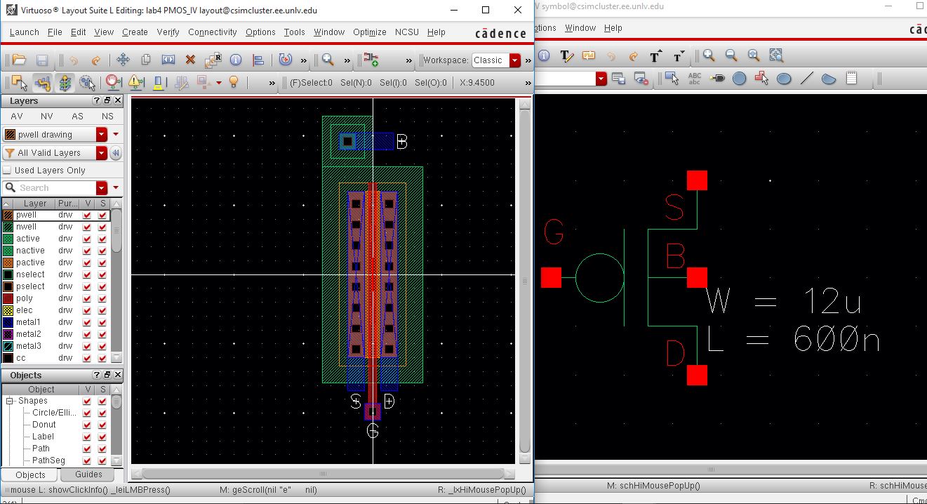
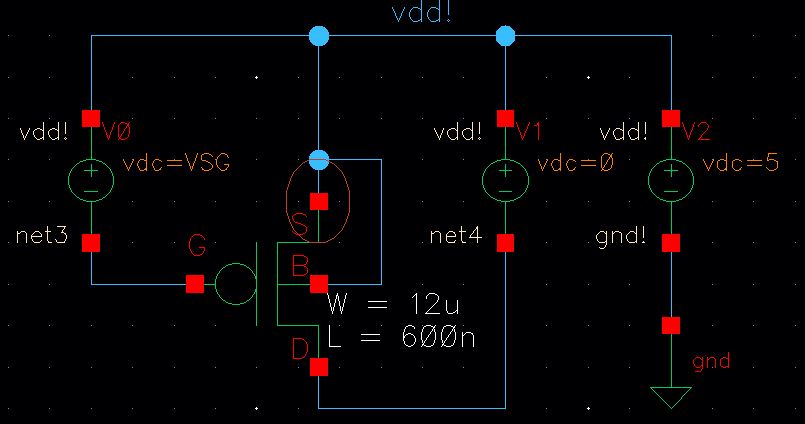
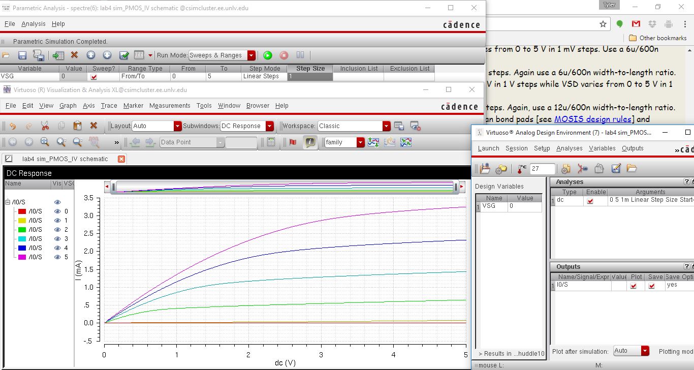
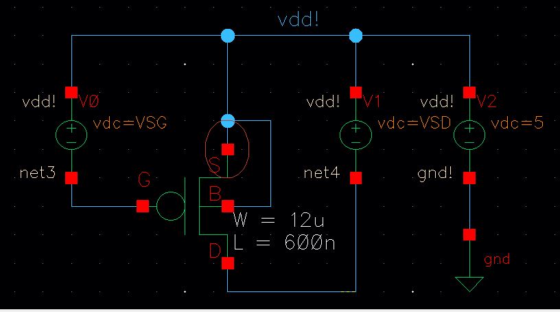
- A
schematic for simulating ID v. VSD (note VSD not VDS) of a PMOS device
for VSG (not VGS) varying from 0 to 5 V in 1 V steps while VSD varies
from 0 to 5 V in 1 mV
steps. Use a 12u/600n width-to-length ratio.
- The schematic and
simulation results using my PMOS device designed in Tutorial 2:
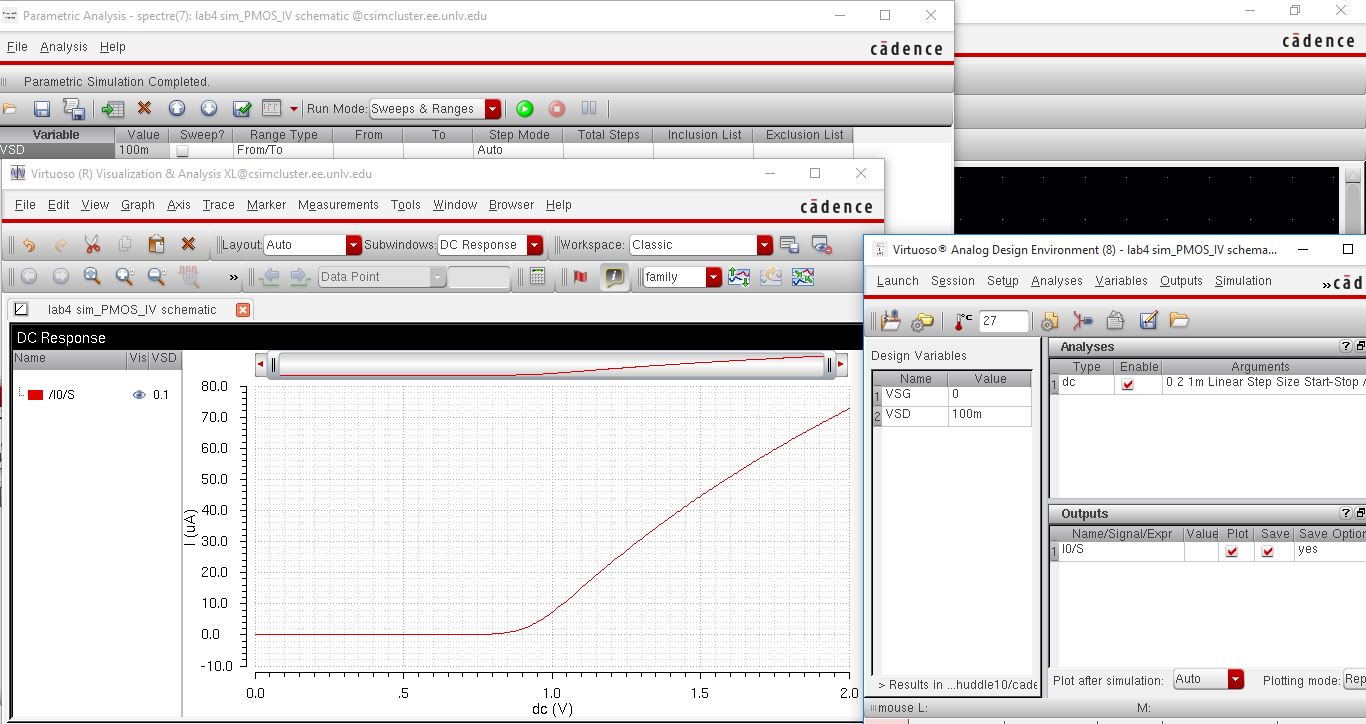
- A
schematic for simulating ID v. VSG of a PMOS device for VSD = 100 mV
where VSG varies from 0 to 2 V in 1 mV steps. Again, use a 12u/600n
width-to-length ratio.
- The schematic and
simulation results using my PMOS device designed in Tutorial 2:
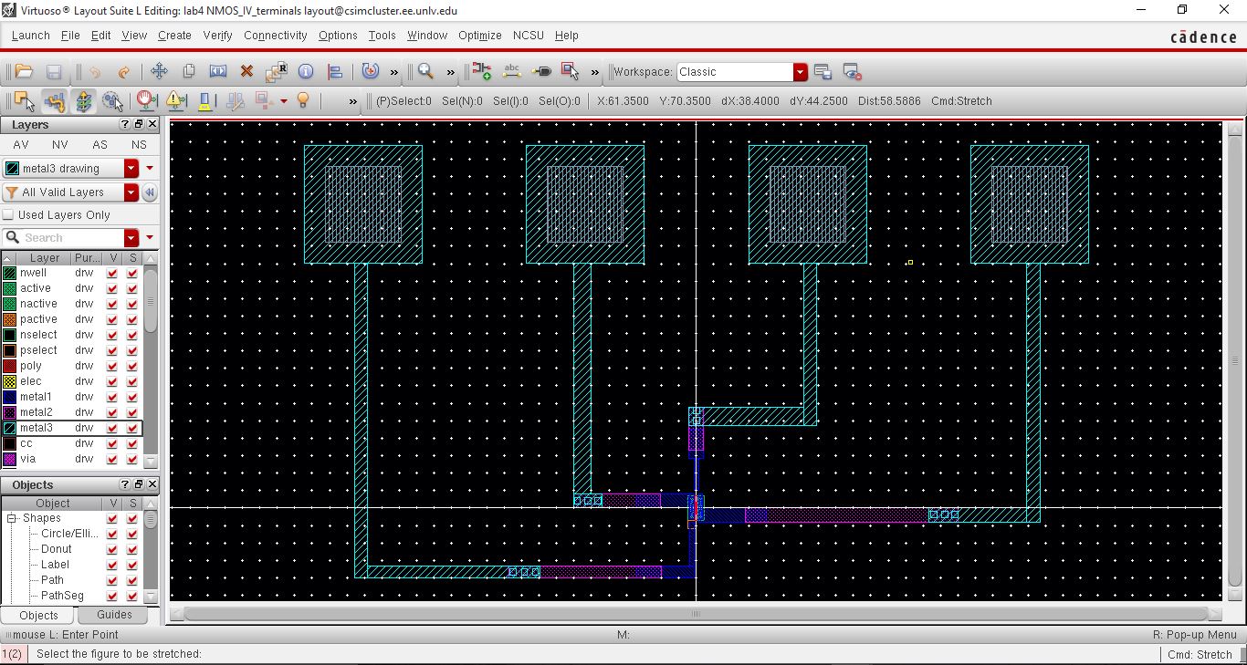
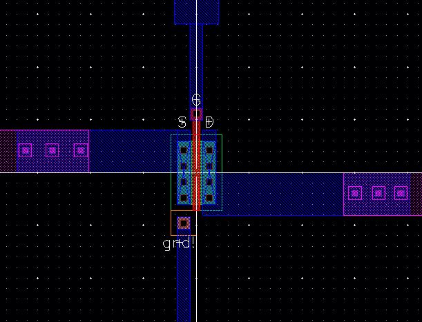
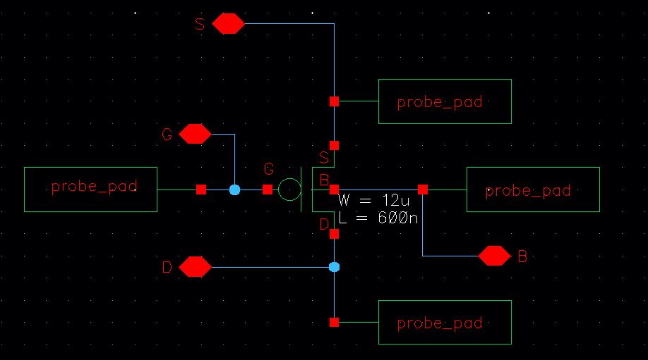
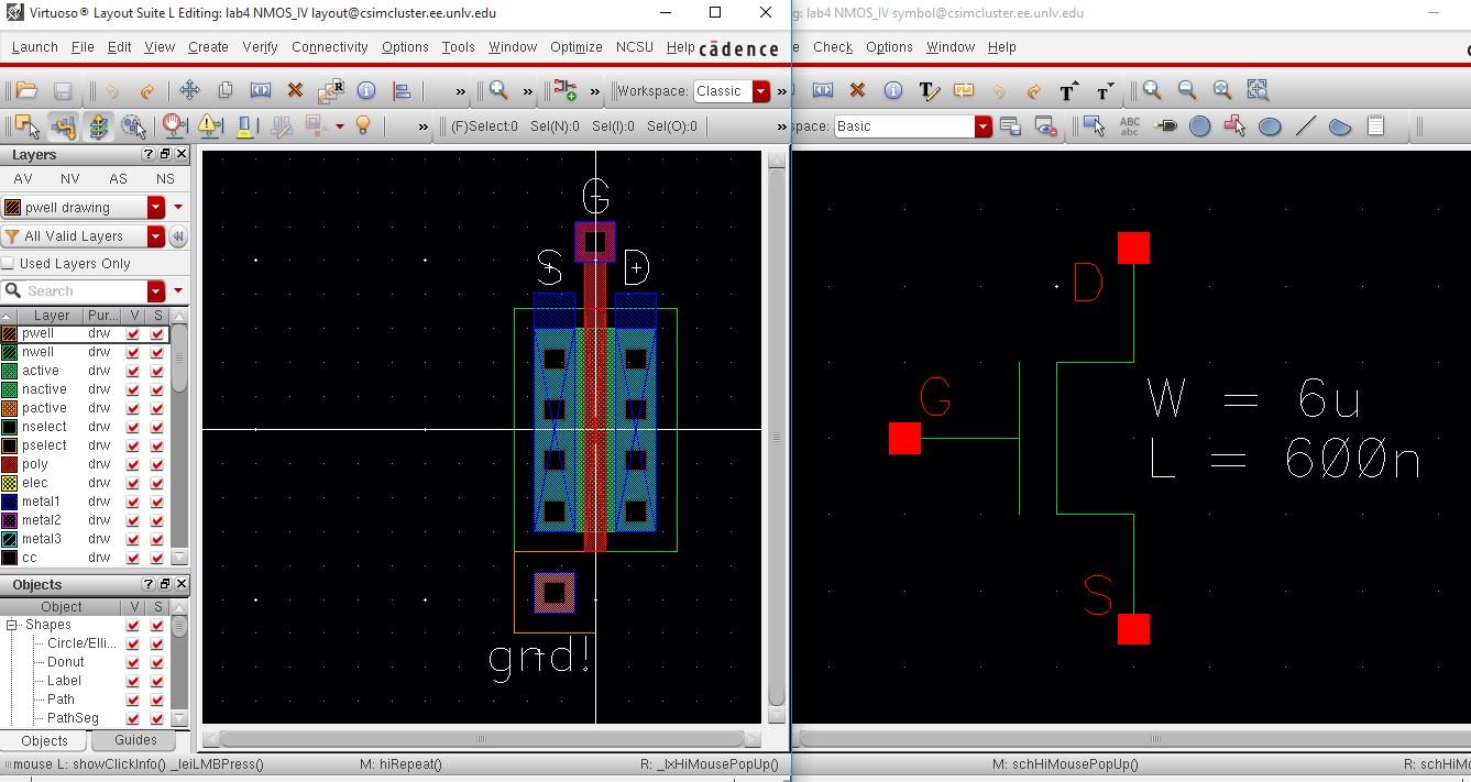
- Lay
out a 6u/0.6u NMOS device and connect all 4 MOSFET terminals to probe
pads (which can be considerably smaller than bond pads [see MOSIS
design rules] and
directly adjacent to the MOSFET (so the layout is relative
small).
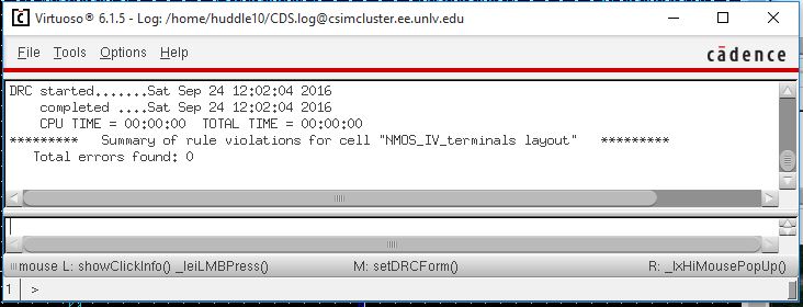
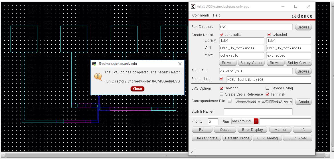
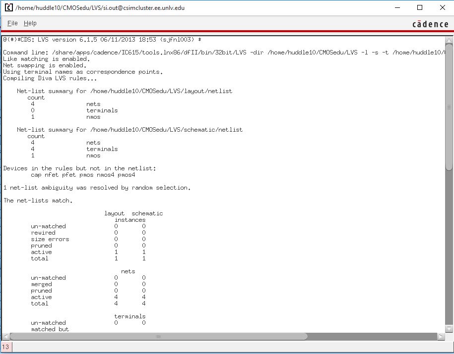
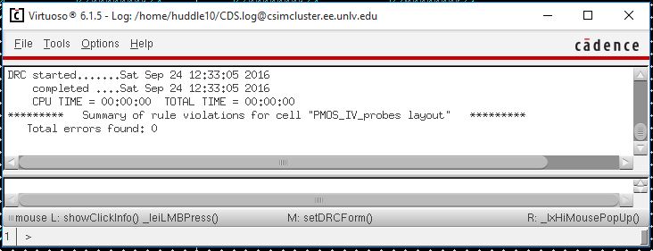
- Show your layout
passes DRCs.
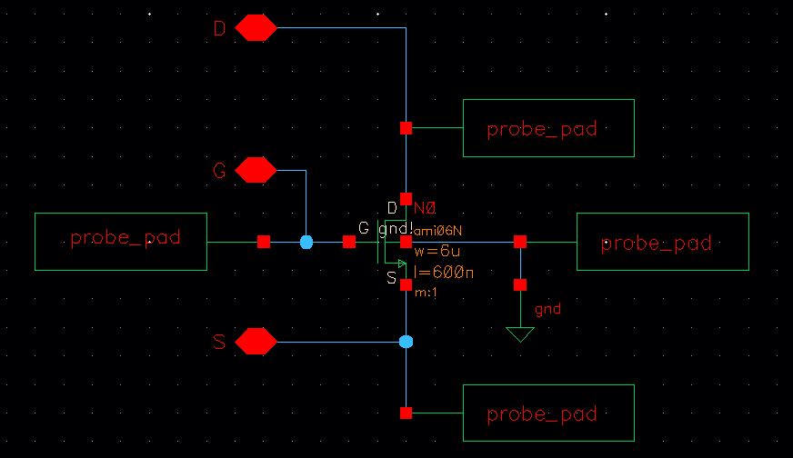
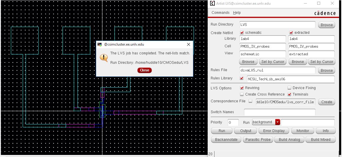
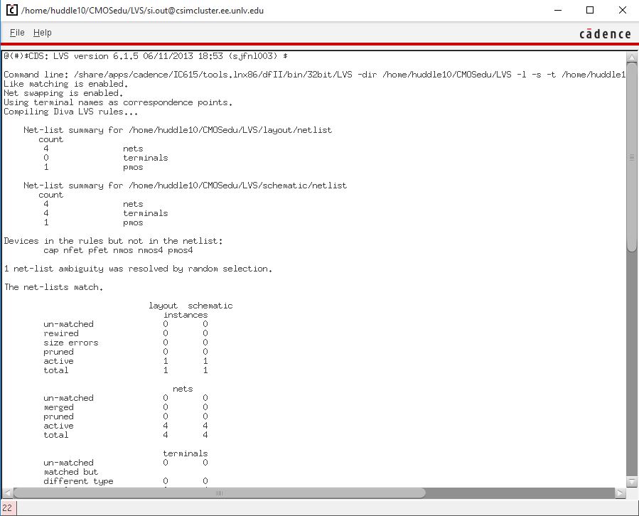
- Make a corresponding
schematic so you can LVS your layout.
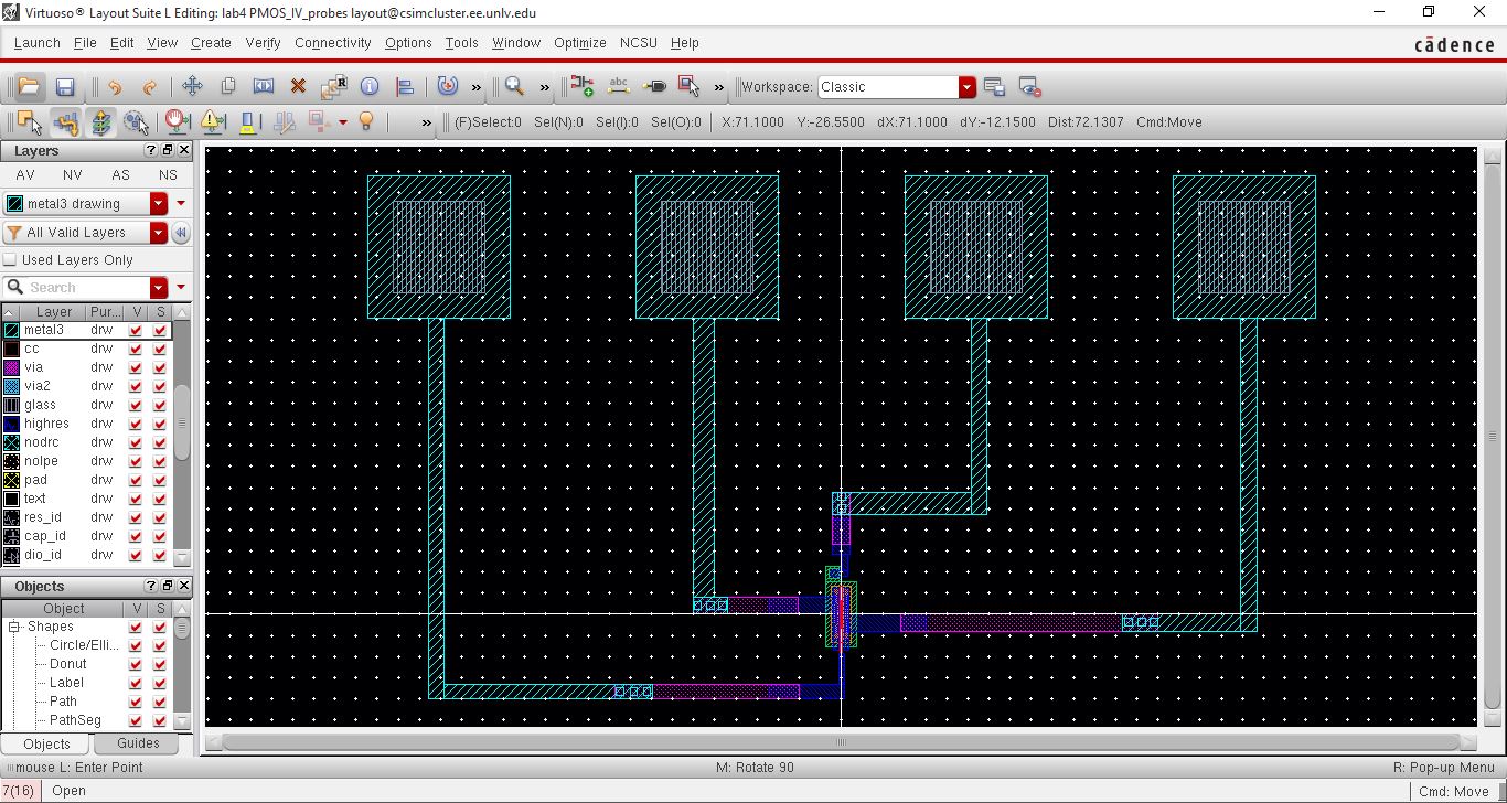
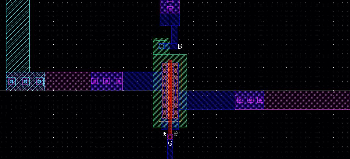
- Lay out a 12u/0.6u
PMOS device and connect all 4 MOSFET terminals to probe pads.
- Show your layout
passes DRCs.
- Make a corresponding
schematic so you can LVS your layout.
Return
to EE 421L Labs
Return
to my Labs Index