Lab 3 - ECE 421L
Designing the 10K n-well resistor
By our design rules, lamda = 300nm.
The minimum n-well width = 12*lamda = 3.6um.
The sheet resistance of n-well = 800 ohms/square.
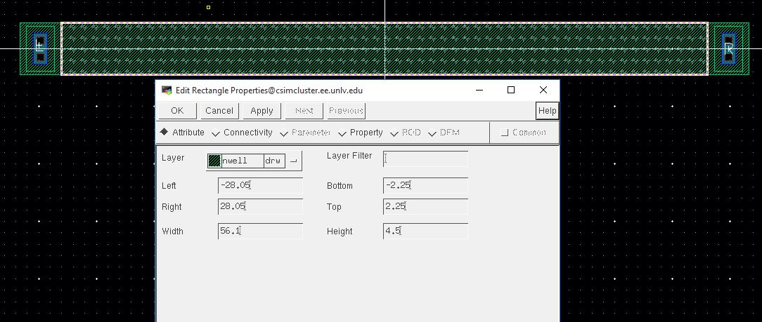
Choose width of 4.5um, thus
L = (R*W)/(Rsquare) = (10K*4.5um)/(800) = 56.1um,
which is rounded to the nearest 0.15um to algin with the grid and pass the DRC verification.
L=56.1um, W=4.5um
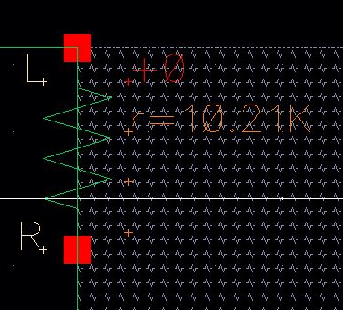
R = 10K confirmation from extracted view
The layout
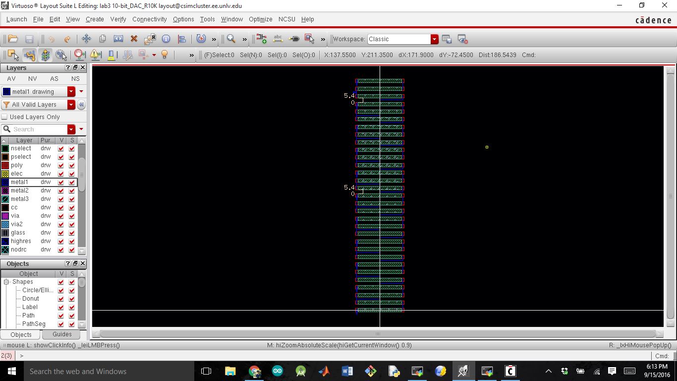
- Each resistor is laid out in parallel in a stack
- The resistors are each a distance of 5.4um between one another
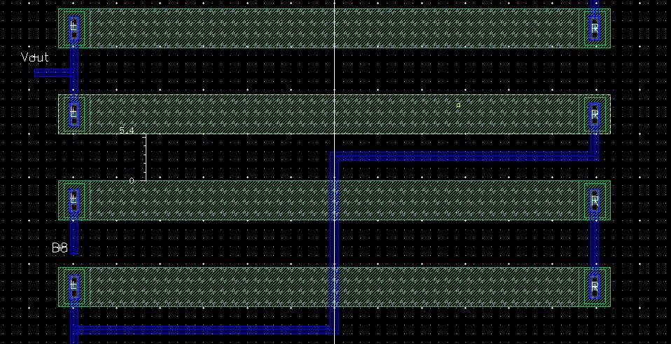
Close up of the layout pattern. Notice the pins are on metal1.
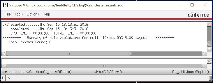
DRC passed.
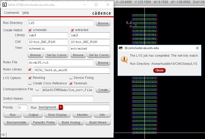
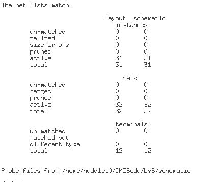
LVS passed.
Link to my design directory here.