
Lab 6 - EE 421L
Design, layout, and simulation of a CMOS NAND gate, XOR gate, and Full-Adder
The zip for this lab containing the cells used can be downloaded here.
Symbol for 2-input NAND gate Symbol for 2-input XOR gate


Ensure gate inputs, outputs, vdd!, and gnd! are all routed on metal1.
The following image shows the layout of the NAND2 gate with a larger cell height to easily route the layout of our full-adder
and to also leave room for more complicated layouts in the future. The DRC passes with no errors here.

Here we can see the extracted view and that the layout of our NAND2 gate passes the LVS.

Now we can see the complete layout of our XOR gate. Luckily, we were able to do all of our connections without the need
for routing anything on metal3. Just like the NAND2 gate, there are no DRC errors for us.

The extracted view of the XOR gate is shown side-by-side with the LVS showing that the layout does indeed match our schematic.

Using Spectre simulate the logical operation of the gates for all 4 possible inputs (00, 01, 10, and 11).
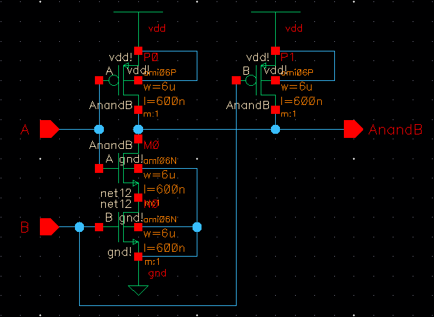
Below is our schematic that was used to simulate the logical operation of our three gates (including the inverter).
The first voltage source has a period that is twice the period of the second voltage source. This will let us count
from 0 to 3 with our input to check all 4 possible inputs. The simulation of the full-adder includes an image that
shows the properties of one of the voltage sources to give a clearer explanation of how this would work.

Here is the truth table for the three outputs Ai, AnandB, and AxorB.

Comment on how timing of the input pulses can cause glitches in the output of a gate.
And here is the simulation representing the graph and logical operation of each of the three gates.
We can see in both the output from the NAND gate and the XOR gate that there is a glitch that occurs at 200ns.
Based on the rise and fall times of our pulses, along with when they are changing from high to low, it can cause
the wrong value to be output from the gate for a very small segment of the output. If the transitions aren't
exact then they will cause these types of glitches.

Using these gates, draft the schematic of the full adder.
Create a symbol for this full-adder.
Below is the schematic of the full-adder with the instantiated symbols create earlier (hopefully my initials are able to be seen).

And this is the symbol view of our schematic that will be used next to simulate the logic operation of our full-adder.
It can be seen placed into the simulation schematic on the right side. There are 3 voltage sources connected to the
full-adder in order to give all possible inputs for a, b, and cin. vdd is set as a global variable within the Stimuli settings
to run at 5V.


My transient simulation runs for 800ns to show the logic operation of the full-adder. The Object Properties window below shows the
properties of the voltage pulse connected to the input, cin. Since the bit of cin will be alternating every set of inputs, the pulse width
is 100ns with a period of 200ns. Even though inputs a and b are not shown, a has a pulse width of 400ns with a period of 800ns and
b has a pulse width of 200ns with a period of 400ns.

To fully understand the simulation and the logic operation of the full-adder, the truth table of the full-adder is shown below.

Finally, we have the simulation of our full-adder, also with the minor glitch seen with both outputs (that was explained
with the first simulation of the NAND and XOR gates). If compared with our truth table, it matches just how it should.

Layout the full-adder by placing the 5 gate end-to-end so that vdd! and gnd! are routed.
Full-adder inputs and ouputs can be on metal2 but not metal3.
DRC and LVS your full-adder design.
Our final layout for this lab is the layout of our full-adder. The gates laid out go in an alternating order of NAND, XOR, NAND, XOR, NAND.
The only routing that needed to be done on metal3 was the output of the first two NAND gates to the input of the third NAND gate.

The DRC of the full-adder is shown below, with zero errors, and in front of the full-adder layout.

