Lab 4 - EE 421L


IV characteristics and layout of NMOS and PMOS devices in ON's C5 process

Michael Ghisilieri

ghisilie@unlv.nevada.edu

9/22/16


Lab Work:


This lab covers laying out NMOS and PMOS devices and simulating circuits using both NMOS and PMOS

to show IV characteristics of various circuits. Extra layouts will also be done to show how an NMOS and

PMOS will look with probe pads connected to each terminal in a layout.


Generate 4 schematics and simulations:


A schematic for simulating ID v. VDS of an NMOS device for VGS varying from 0 to 5 V in 1 V steps while

VDS varies from 0 to 5 V in 1mV steps. Use a 6u/600n width-to-length ratio. 


IDvsVDS_sch.jpgIDvsVDS_sim.jpg


A schematic for simulating ID v. VGS of an NMOS device for VDS = 100 mV where VGS varies from

0 to 2 V in 1 mV steps. Again use a 6u/600n width-to-length ratio.  


IDvsVGS_sch.jpgIDvsVGS_sim.jpg


A schematic for simulating ID v. VSD (note VSD not VDS) of a PMOS device for VSG (not VGS) varying from

0 to 5 V in 1 V steps while VSD varies from 0 to 5 V in 1 mV steps. Use a 12u/600n width-to-length ratio. 


IDvsVSD_sch.jpgIDvsVSD_sim.jpg  


A schematic for simulating ID v. VSG of a PMOS device for VSD = 100 mV where VSG varies from

0 to 2 V in 1 mV steps. Again, use a 12u/600n width-to-length ratio.  


IDvsVSG_sch.jpgIDvsVSG_sim.jpg  


Layout a 6u/0.6u NMOS device and connect all 4 MOSFET terminals to probe pads:

Make a corresponding schematic so you can LVS your layout.


The first image is the nmos4 component connected to 4 probe pads and the connections are shown in the zoomed layout on the right. 

nmos_probe_sch.jpgnmos_probe_zoom.jpg


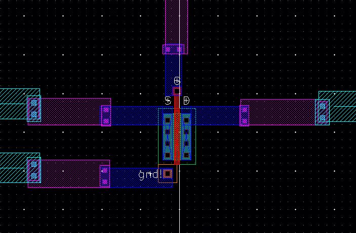
The full layout below shows that the NMOS is in fact connected to the probe pads (21um x 33um).


nmos_probe_lay.jpg


Show your layout passes DRCs.


These images show that the NMOS layout with probe pads does in fact pass DRC with zero errors found as well as

being able to pass the LVS once the layout has been extracted.


nmos_probe_drc.jpgnmos_probe_lvs.jpg


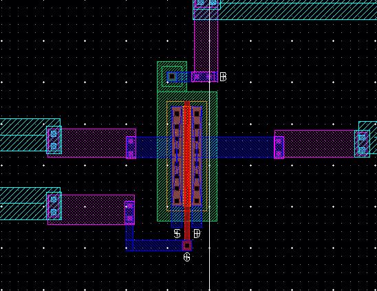
Layout a 12u/0.6u PMOS device and connect all 4 MOSFET terminals to probe pads:

Make a corresponding schematic so you can LVS your layout.  


The first image is the pmos symbol (created in the pre-lab) connected to 4 probe pads and the connections are shown in the zoomed layout on the right. 


pmos_probe_sch.jpgpmos_probe_zoom.jpg


With some adjustments and rerouting of the metal1 and metal2 layers, the PMOS was easy to fit into the same layout that the NMOS

was originally used in and this can also be extracted to LVS with our new PMOS circuit.


pmos_probe_lay.jpg


Our second layout does indeed pass DRC with no errors found and once again the LVS for our PMOS cell passes successfully.


pmos_probe_drc.jpgpmos_probe_lvs.jpg


Return to EE 421L Labs