Project - EE 421L
Tyler Ferreira,
ferret1@unlv.nevada.edu
November 15, 2016
Project
- design a circuit that takes a serial input and detects (outputs
a high logic signal called detect) the sequence 101011
The inputs to your circuit are clk and in
Make sure that the output of your design, detect, is buffered before connecting to a pad
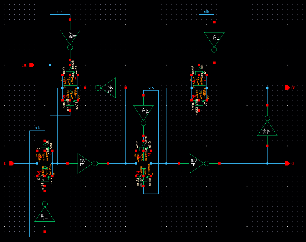
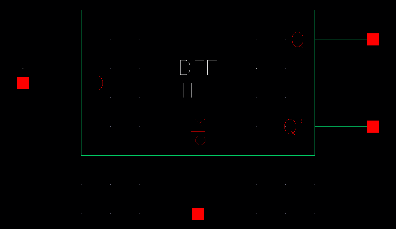
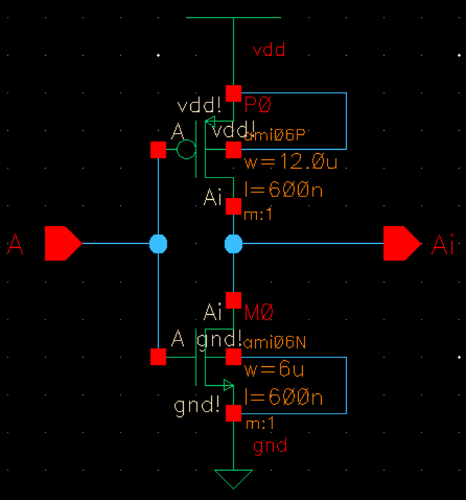
For the first part of the project I will create a schematic and a symbol for the data flip flop.
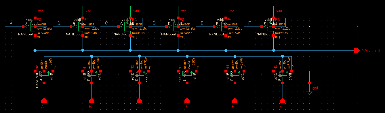
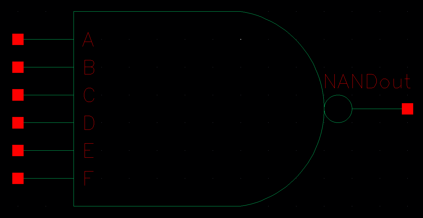
Now I will create a 6-bit NAND gate for use in the detector circuit.
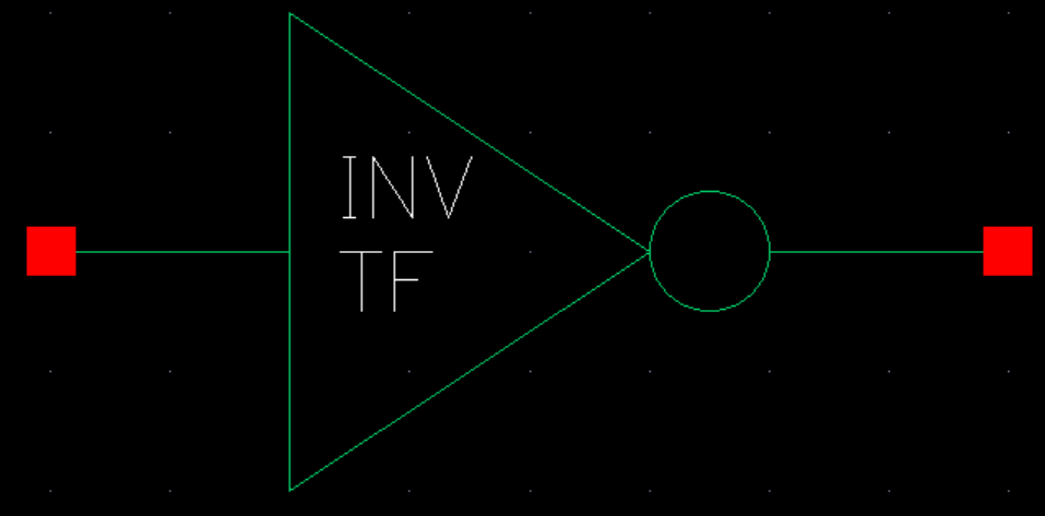
Schematic and symbol for the inverter used in my design:
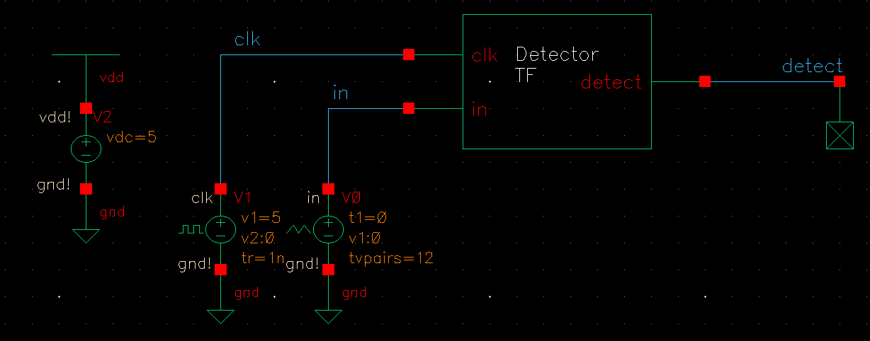
Now that I have all of my components for the detector circuit I will put them all together.
Since I need to detect a 6-bit binary number I will need 6 D flip flops.
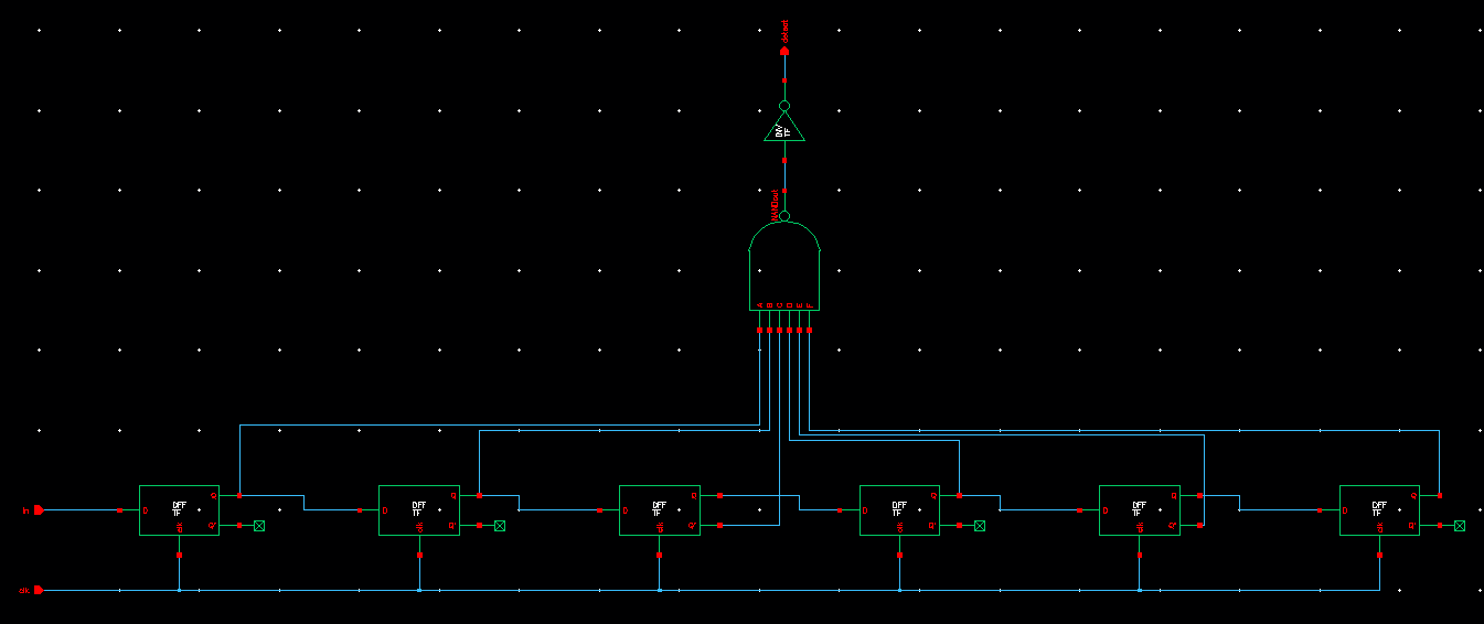
The
inputs into the NAND gate are connected to the Q or Q' of the D flip
flops. Since we are detecting 101011 A will be connected to Q, B will
be connected to Q, C will be connected to Q', D will be connected to
Q, E will be connected to Q',
and F will be connected to Q. The Q
will represent the 1s in our sequence and the Q' will represent the 0s
in our sequence. Now that I have a schematic I will create a symbol for
it.
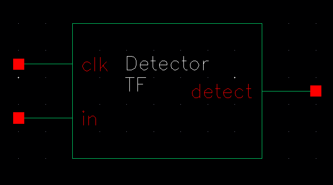
Now
I will use this symbol to create a schematic to simulate the operation
of the detector circuit. I will use a piecewise linear voltage source
to test different sequences of numbers.
The simulation results for an incorrect sequence:
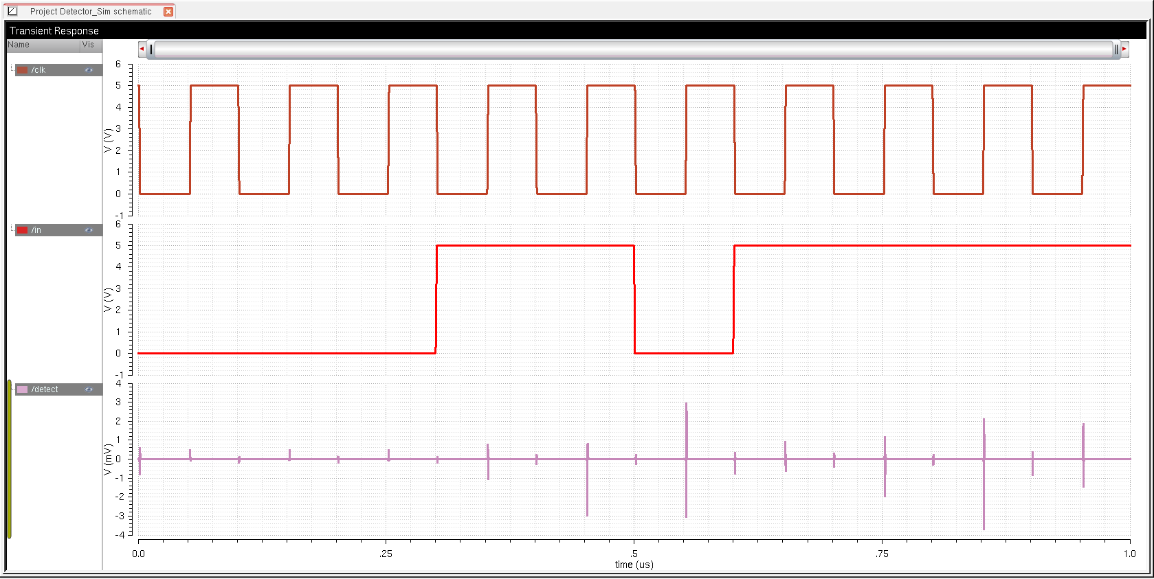
Since the sequence was not received the output will remain at logic low.
The
small spikes in voltage in my output signal will not cause a logic
error because the spikes are only a few mV in amplitude. This is not
large enough to affect the logic at the output.
The simulation results for a sequence containg 101011:
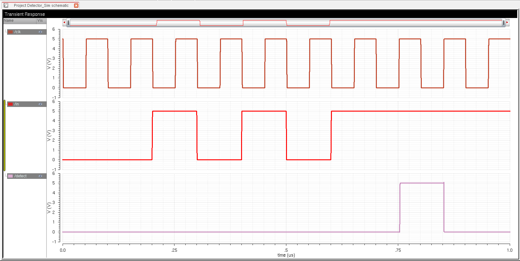
This sequence contains our target sequence 101011 and when it receives it the output goes to logic high.
The second part of this project is to layout the detector for use in our chip project.
First I will layout each piece of the detector circuit individually.
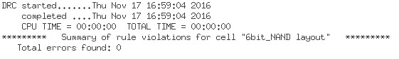
Here is my layout for the 6bit NAND gate:
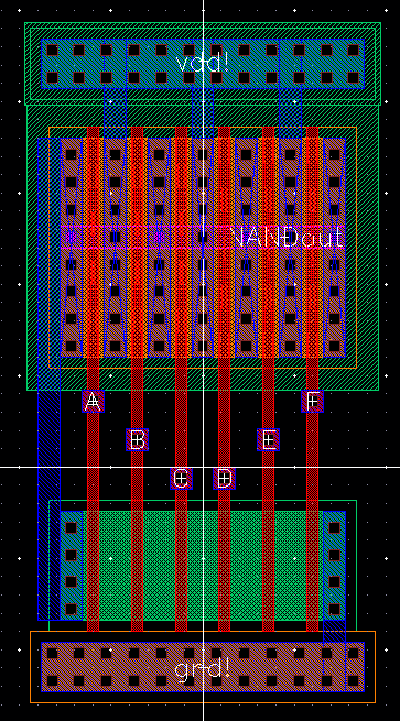
I will verify my 6bit NAND gate layout:

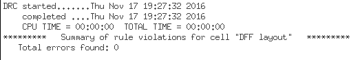
Now I will layout my data flip flop:

Verification for my DFF layout:

Layout for my inverter:
Verification for my inverter layout:

Now
that I have finished the layouts for the 6bit NAND gate, the DFF, and the inverter I
will connect them together to create my detector layout.
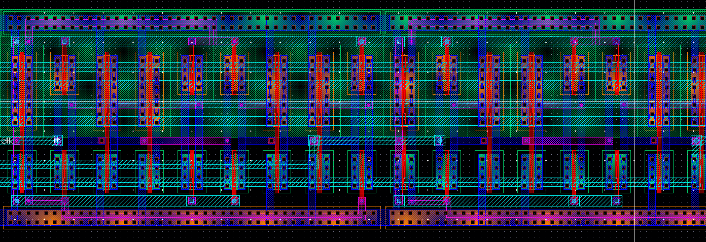
In my detector layout I will instantiate my 6bit NAND layout, 6 of my DFF layouts, and my inverter layout.
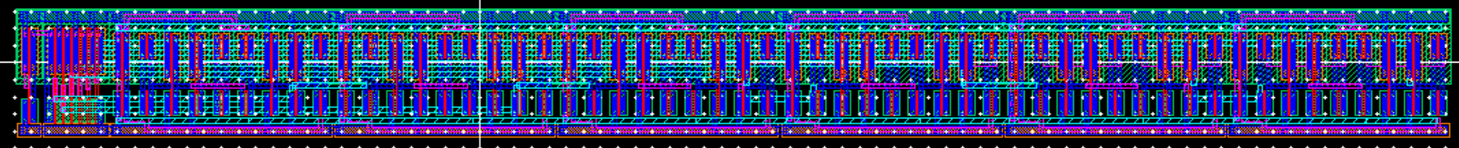
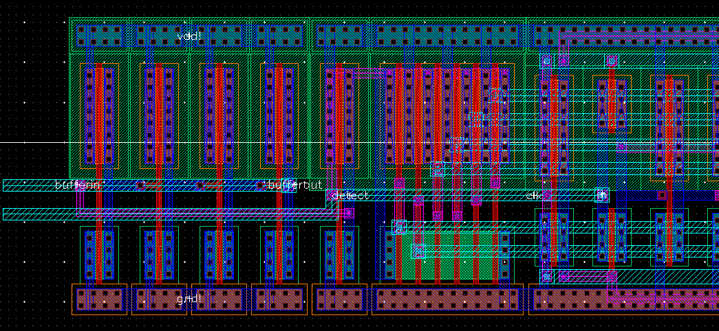
Here is an image of my entire layout:
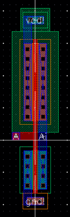
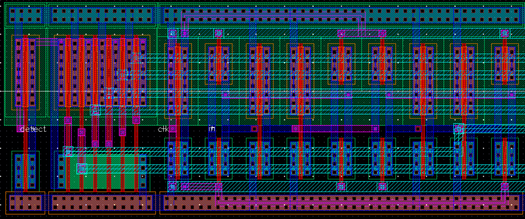
Here is a zoomed in image of the NAND gate, inverter, and the first DFF:
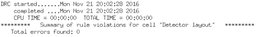
Verification for my layout:

Connecting a buffer on the output of the inverter to connect to a pad:
Now I will simulate my extracted view using an incorrect sequence as well as a correct sequence.
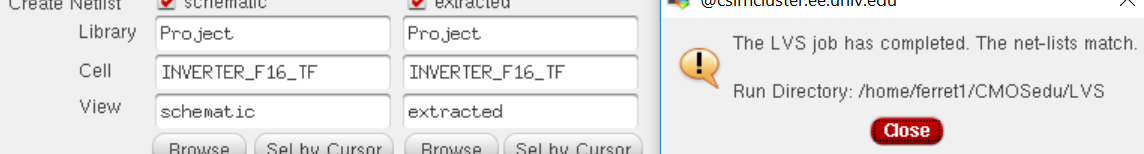
Netlist showing that I used my extracted view:
Simulation with incorrect sequence:
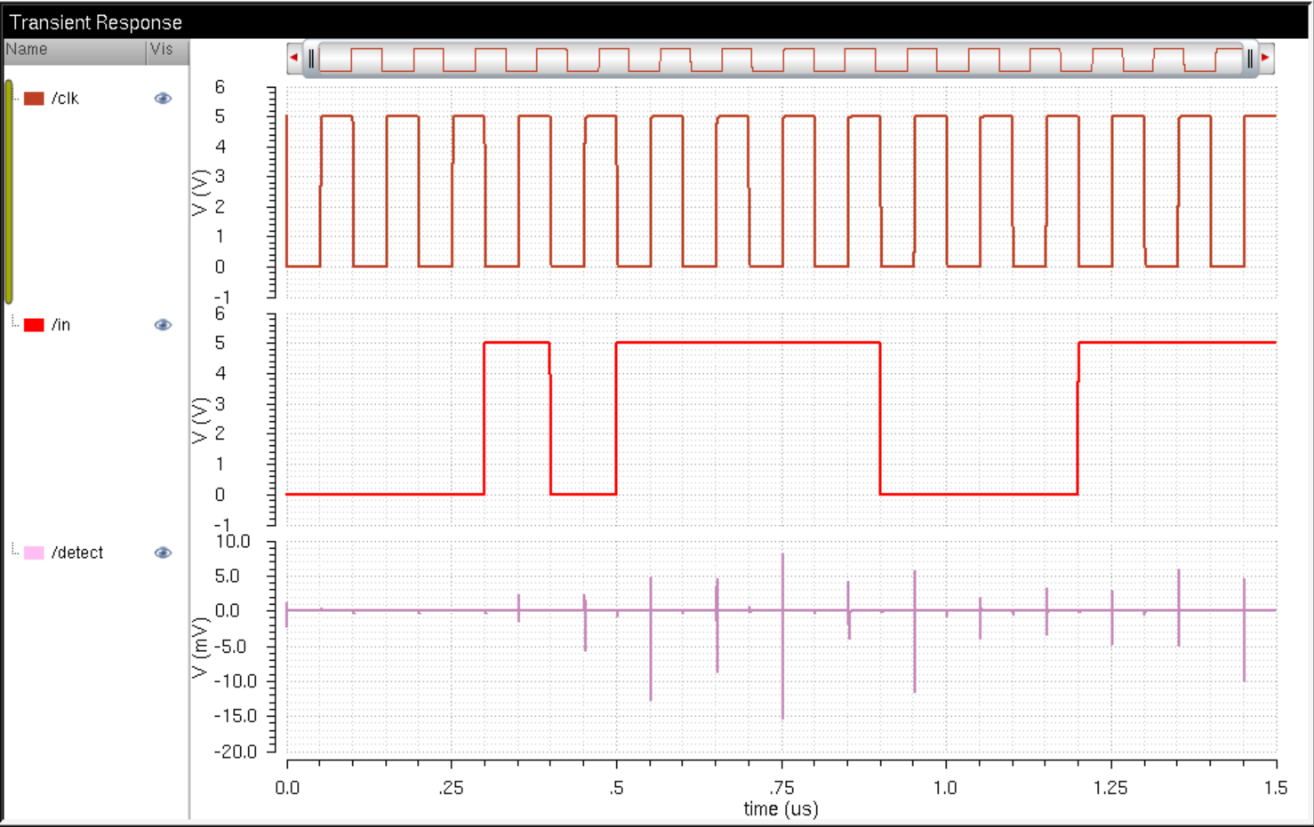
The spikes of voltage in my output are so low that they will not affect the logic of my output.
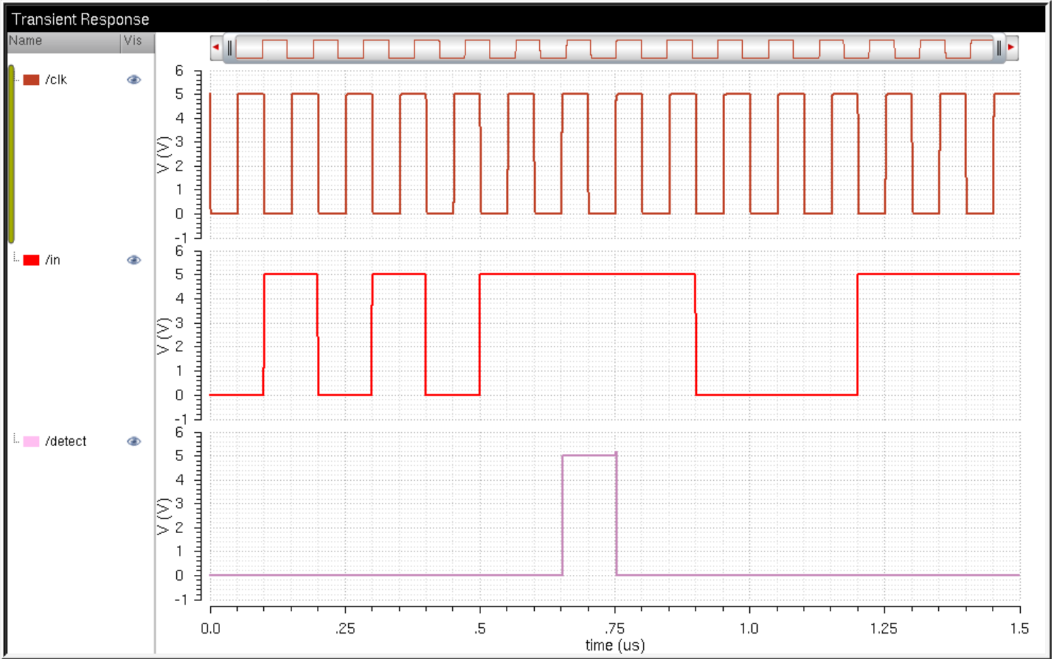
Simulation with correct sequence:
Link to download schematics and layouts for this project: Project.zip
Return to EE 421L Labs