Lab 3 - EE 421L
deignank@unlv,nevada.edu
9/21/16
Pre-lab:
I used google drive to backup all my files for lab 3 as shown
below:

10K n-well Resistor:
To layout a
resistor, I first added a rectangle with the n-well layer. The length and width
of the rectangle is what dictates the resistance of the component. The equation
to relate total resistance to the length and width is R = Rsquare*l/w.
The Rsquare for our process is approximately 800
ohms. To make a 10K resistor we have to choose a ratio of length to width that
will equal 10K when multiplied by 800. These values also have to snap to the
.15 micrometer grid. The minimum width for our process is 3.6 micrometers. Choosing
the length and width as 4.5 micro and 56 micro follow all of these constraints.
After creating
the n-well rectangle, ntaps have to be added to the
ends so that pins can be attached. The n-tap is a component in the ami06 tech library.
After adding the n-tap, metal pins had to be added to the contact points. The
finished layout is shown below:

After passing
the DRC I extracted the layout. Opening the extracted layout allows for the
resistance to be viewed. The extracted view is shown below:

As shown above
the total resistance is 10.24K. This is within the allowed error.
DAC Layout:
I used the
n-well resistor to create the layout of the DAC. Creating an instance and
navigating to the library where I created the n-well resistor allowed me to use
it as a component. Thirty-one of these resistors were needed for the DAC layout.
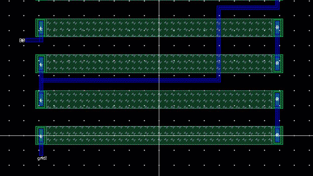
Two resistors in series and one in parallel were needed for each bit of the DAC,
with one extra one for the last bit. Metal 1 had to be added to connect the
resistors the correct way and to create pins. The image below shows the layout for one bit
of the DAC:

Creating
copies of the layout above and pasting allowed for completion of the entire DAC
as shown below:

DRC and LVS
were passed as shown below:


I was able to
run the simulation using the layout instead of the schematic. Using the layout
gave the waveform shown below, which matches the waveform from the original
schematic.

I backed up my
files after completing the above lab with google drive as shown below:
