Lab Project - ECE 421L 

Authored by Dominique Anguiano,

Email: anguian3@unlv.nevada.edu

Schematics were completed on November 11,  2016

Layouts were completed on November 18, 2016 


The directory containing all files for this project may be found here.   


 Design, Layout and Simulation of a Detector


Operation of the Detector

  The final project for this lab had us design a detector circuit.  This dectector will accept a 6-bit serial input and compare it to a predefined sequence.  Ifthe input sequence matches, the detector w ill output a signal verifying the match and will continue to do so until a new bit is receieved.  In order to create the device,  two main components are needed: a D Flip-Flop, and a 6-bit AND gate.  Having the D Flip-Flop allows us to store a bit and by having six of these Flip-Flops allows us store the six bit sequence that received at the input of the detector.  These six bits could then be routed into an AND gate which would output a signal if the expected six bit sequence was received. 


Creation of the D Flip-Flop 

 In order to create a D Flip-Flop, we require both transmission gates and inverters.  The transmission gates are necessary as they allow the signal to be synced to a clock as well as allowing the signal to maintain a low level of noise.  The inverters are necessary as they can be used to create a buffer which helps store the value in the device.  The device can be seen in the shematic below.


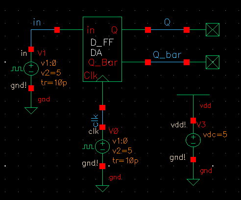
Operation of the D Flip-Flop

The Flip-Flop receieves a signal from the input terminal which can be see on the schematic below.  This signal is not allowed to enter the flip-flop until clock sends a value of "0" and allows the signal to enter into the first section.  When a value of "1" is received, the first Transmission Gate shuts off and captures the signal in the first section also at the same time, the second Transmission gate (seen at the top left of the schematic) turns on and allows the signal to flow in between the two inverters.  These inverters act as a buffer and store the signal until a the clock changes from "0" to "1" again.  When this happens, the third transmission gate turns on and allows the signal from the inverters to flow to the right side of the schematic to the next pair of inverters.  When the signal changes back to "0", the third transmission gate shuts off and the fourth turns on which allows the signal to pass through the second pair of inverters.  This stores the input signal on the right side of the schematic and allows it to be output at Q and Q_bar.  Q_bar is the compliment of the input signal.  


D Flip-Flop schematic

DFF_schematic.PNG


D Flip-Flop Symbol
 
DFF_symbol.PNG


Simulation of the D Flip-Flop


dff_sim_schematic.PNG  dff_sim_results.PNG


 Transmission Gate Schematic and Symbol

 The transmission gate seen in the following schematic was used in the creation of the D Flip-Flop.  This gate was used as it allows a signal to pass through with minimal noise. 


TG_schematic.PNG  TG_symbol.PNG


  Inverter Schematic and Symbol

 The following is the inverter that was used in the creation of the D Flip-Flop, 6-bit AND and buffer


inverter_schematic.PNG  inverter_symbol.PNG


 Creation of the 6-bit AND gate

  The 6-bit and gate follows a similar structure to the 2-bit and gate we used throughout the course.  The main difference is obviously the amount of inputs needed.  For a 6-input AND gate, 6 PMOSs and NMOSs are needed.  The NMOS devices are connected serially and the PMOS devices are connected in parallel.  The schematic and symbol of the device can be seen below.

and_schematic.PNG and_symbol.PNG


 Simulation of the six-bit AND

 The six-bit AND gate functions similarly to the two-bit AND gate in that if any of the inputs recieves a value of "0" the output of the AND gate will output a value of "0"as well.  The simulation shows a scenario where all of the inputs except for one are tied to a value of "1".  The last input alternates between "0" and "1" to change the output of the AND gate.  As we can see from the simulation results below, the device functions as expected and switches outputs when the last input switches.


 and_sim_schematic.PNG  and_sim_results.PNG


Creation of the Buffer
 The buffer is assumed to be driving a load of 20pF.  This load was chosen based on the load requirement in Lab 8 since a buffer in that lab was also driving a 20pF capacitive load.  Knowing this, it becomes fairly simple to calculate the number of required buffers with the following formula.

N = (1/2)*ln(Cload/Cin) => 1/2 * ln(20pf/(3/2)27fF
3 Stages

N.B. This forumla assumes that a gain of 8 is used.

Knowing this information, the schematic and symbol of the buffer can be seen below.  It should be noted that an extra inverter was added in order to ensure that the input signal is the same as the output signal of the buffer.  If the extra inverter was not present, the output would be the inverse of the input.

buffer_schematic.PNG  buffer_symbol.PNGbuffer_symbol.PNG
 

Simulation of the buffer

As we can see from the simulation of the buffer, the output is the same as the input.
 
buffer_sim_schematic.PNG buffer_sim_results.PNG


Creation of the Detector
 The detector circuit can be seen below.  The six flip flops it contains each propagate its signal to the one that follows on every rising rising edge of the clock.  The outputs of each of these flip flops are the compared to the sequence 101011.  This can be seen in the circuit because of the terminals that the AND gate is connected to.  For the terminals that are connected to 'Q_Bar', the bit that is expected on that flip flop is '0'. The terminal is connected to Q_Bar in order to provide the value '1' to the AND gate.  This is to ensure that the AND gate is able to turn on.  If the terminal was connected to 'Q' instead, the AND gate would recieve a '0' which would not allow the AND gate to output true when the correct sequence was received as an input.

detector_schematic.PNG
 
Detector Symbol

detector_symbol.PNG

Simulation of the detector
The detector was configured to expect the sequence 1,0,1,0,1,1.   The simulations were performed using the schematic seen below.

detector_sim_schematic.PNG
 

The marks on each input waveform are the spots at which the sequence occurs.

 detector_sim1.PNG  detector_sim2.PNG

  As we can see from the simulations, the input that occurs before the sequence occurs does not matter and does not influence the detection of the sequence.  Also we can see that the detect signal goes back to being "0" once a new value is read in.  This is because each of the bits is propagated which causes the sequence to no longer match.

This is the end of part 1.


 Layouts

The layout of every device used in the schematic of the sequence detecting circuit can be seen below.


Inverter Layout and Extracted view


Inveter_Layout.PNG  Inverter_Extracted.PNG


Transmission Gate Layout and Extracted view


TG_DRC.PNG   TG_Extracted.PNG


AND Gate Layout and Extracted view

   Here is the layout of the six-bit AND gate, with the DRC results

AND_DRC.PNG


And here is the Extracted View of the AND gate with the LVS results


AND_LVS.PNG


 Buffer Layout and Extracted view

    Here is the layout of the buffer with the DRC Results   

Buffer_DRC.PNG


Here is the wonderful extracted view 


 Buffer_DRC.PNG


Since the LVS result did not fit in the former screenshot without it looking awkward, here it is as a seperate image


Buffer_LVS.PNG


 D Flip-Flop Layout and Extracted view

     Here is the wonderful Layout of the D Flip Flop

DFF_DRC.PNG


   And here is the extracted view.

DFF_Extracted.PNG


 And of course, we can't forget to show the LVS result.


DFF_LVS.PNG


Sequence Detector Layout and Extracted view
    Here is the end result of combining all of the other devices together to create the sequence detector.
  
Detector_Layout.PNG


 The Extracted view can be seen below.

 Detector_Extracted.PNG


And here is the LVS result to ensure that the layout matches the schematic.


DFF_LVS.PNG


 This concludes the lab project.


Return to EE421L Labs