Lab 4: IV Characteristics and Layout of NMOS and PMOS devices in ON's C5 Process - EE 421L
Authored By: Joey Yurgelon
Email: yurgelon@unlv.nevada.edu
September 20th, 2015
Pre-lab Work:
- Back-up all of your work from the lab and the course.
- Read through this lab before starting it.
- Go through Tutorial 2 seen here.
- In
the simulations in this lab the body of all NMOS devices (the
substrate) should be at ground (gnd!) and the body of all PMOS devices
(the n-well) should be at a vdd! of 5V.
Exercise #1: Go through Tutorial #2
- Below
is a list a few of the milestones as I ventured through Tutorial 2. The
purpose of the tutorial was to teach one how to layout a PMOS/NMOS in
the C5 process, and then attach a schematic to create a 1v1
correspondance between the layout and schematic. This lab will make use
of the mosfets developed in this tutorial. The NMOS simulations and LVS
are on the left hand column while the PMOS are on the right.
Lab Description:
- Students
will simulate and layout PMOS/NMOS in C5 process.
Lab Requirements:
- Generate
4 schematics and simulations (see the examples in the Ch6_IC61 library,
but note that for the PMOS body should be at vdd! instead of gnd!):
- A schematic for simulating ID
v. VDS of an NMOS device for VGS varying from 0 to 5 V in 1 V steps
while VDS varies from 0 to 5 V in 1 mV steps. Use a 6u/600n
width-to-length ratio.
- A
schematic for simulating ID v. VGS of an NMOS device for VDS = 100 mV
where VGS varies from 0 to 2 V in 1 mV steps. Again use a 6u/600n
width-to-length ratio.
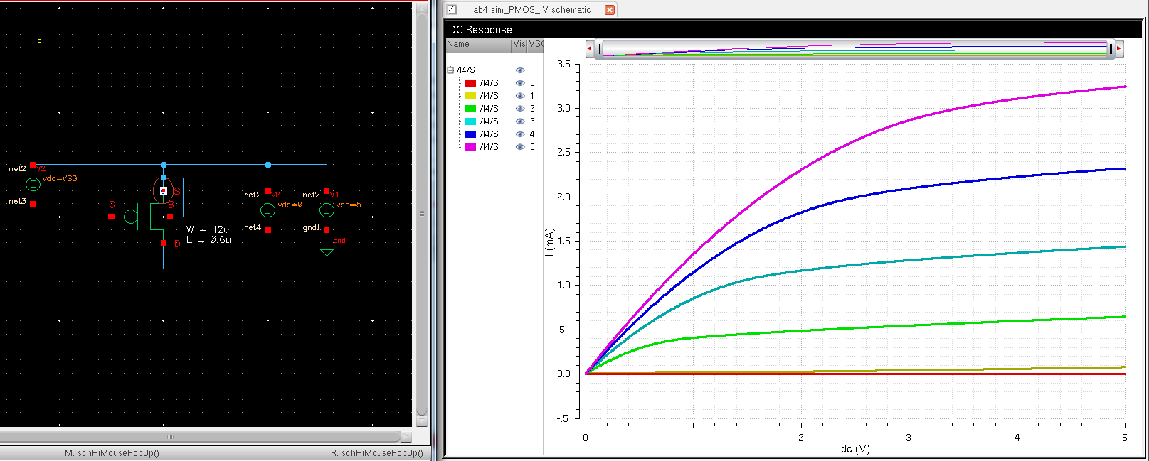
- A
schematic for simulating ID v. VSD (note VSD not VDS) of a PMOS device
for VSG (not VGS) varying from 0 to 5 V in 1 V steps while VSD varies
from 0 to 5 V in 1 mV steps. Use a 12u/600n width-to-length ratio.
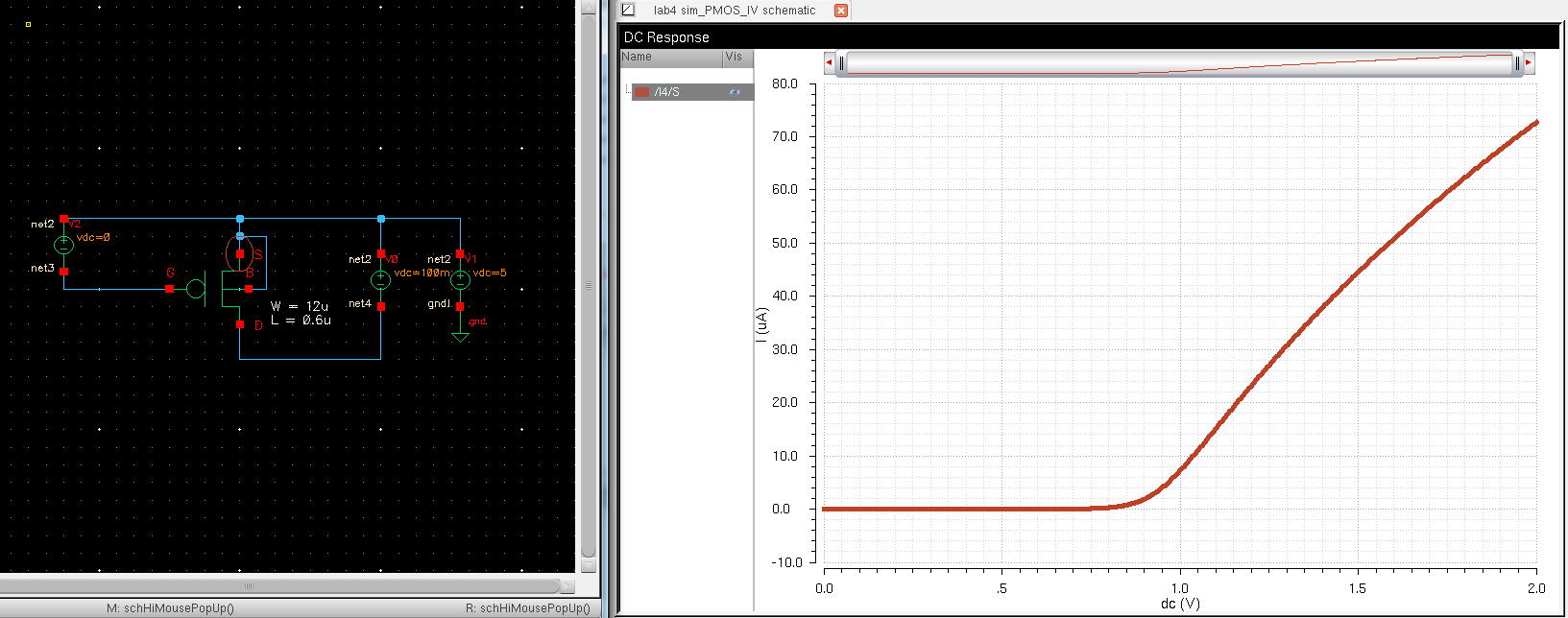
- A
schematic for simulating ID v. VSG of a PMOS device for VSD = 100 mV
where VSG varies from 0 to 2 V in 1 mV steps. Again, use a 12u/600n
width-to-length ratio.
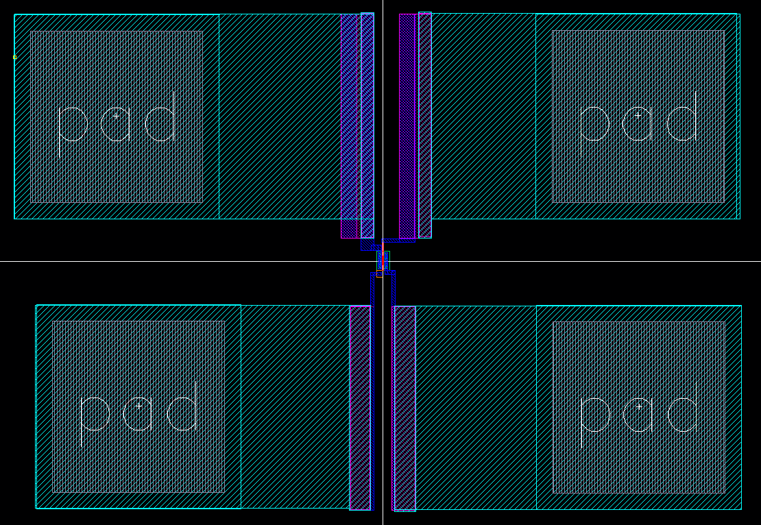
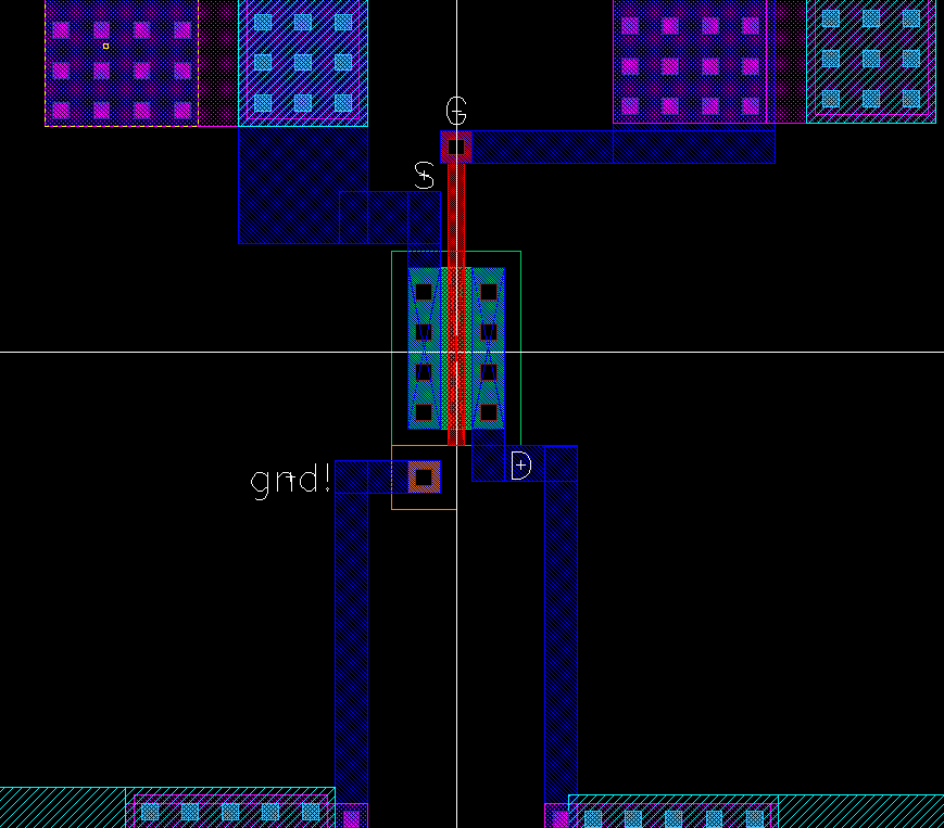
- Lay
out a 6u/0.6u NMOS device and connect all 4 MOSFET terminals to probe
pads (which can be considerably smaller than bond pads [see MOSIS design rules] and directly adjacent to the MOSFET (so the layout is relative small).
- Show your layout passes DRCs.
- Make a corresponding schematic so you can LVS your layout.
- Lay out a 12u/0.6u PMOS device and connect all 4 MOSFET terminals to probe pads.
- Show your layout passes DRCs.
- Make a corresponding schematic so you can LVS your layout.
- Some examples are seen below (click for a larger view).
- They
are, in order: 1) probe pad layout, 2) probe pad schematic, 3) probe
pad symbol, 4) schematic of the MOSFET with probe pads, 5)
corresponding symbol view, 6) corresponding layout (which is DRCed and
LVSed), 6) zoomed in view of the layout, and finally 7) simulation
schematic for ID v VSD for varying VSG (which is not used for an LVS
since there is no way to lay out a battery).
- ALL OF THE DESIGN FILES ASSOCIATED WITH THIS LAB CAN BE FOUND HERE.
Experimental Results:
Exercise #1:
Generate 4 schematics and simulations (see the examples in the Ch6_IC61
library, but note that for the PMOS body should be at vdd! instead of
gnd!)
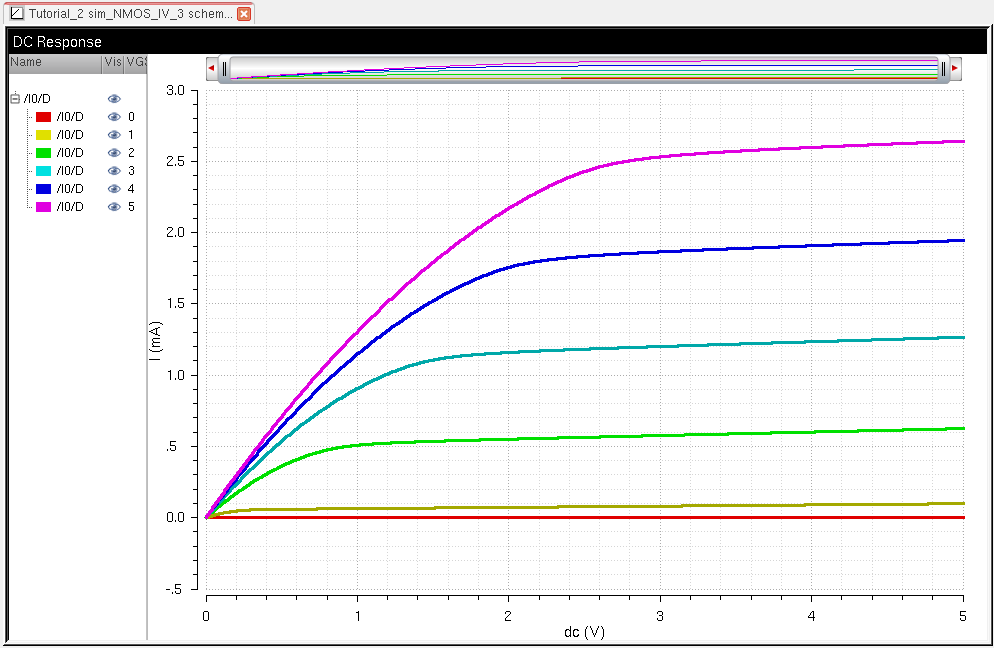
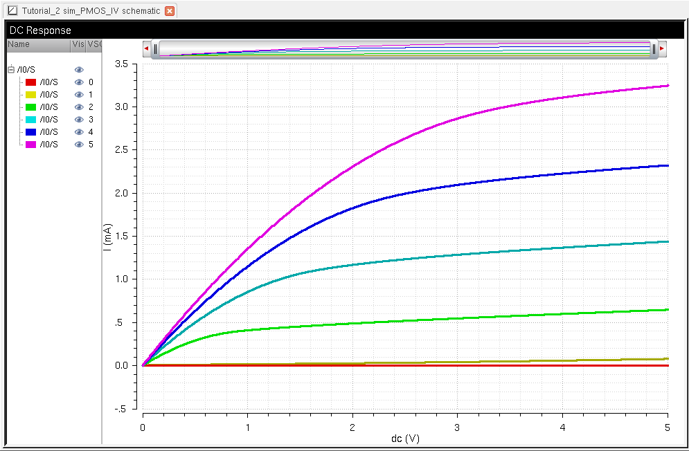
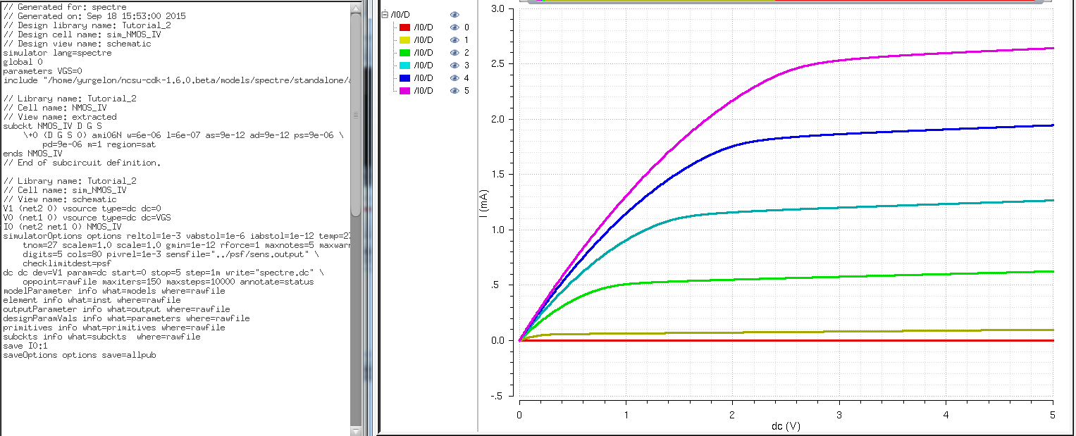
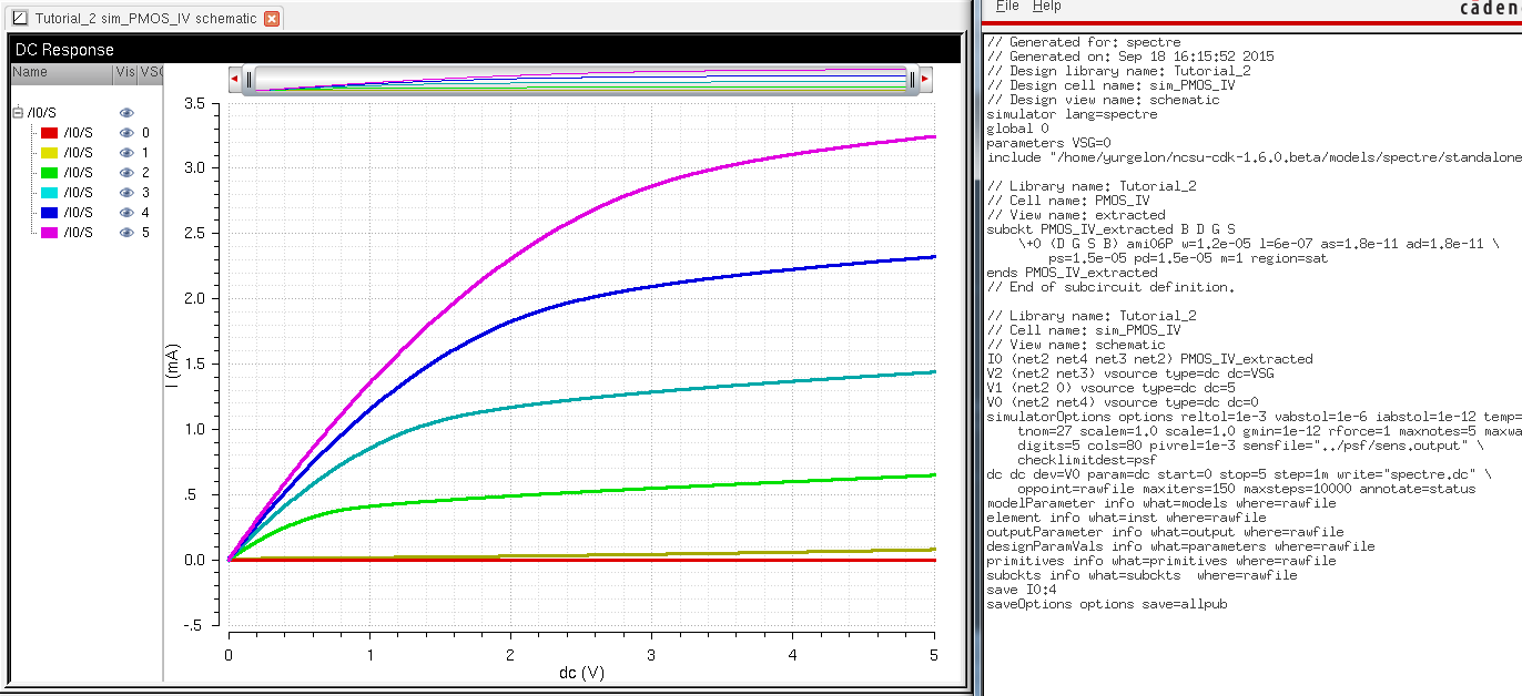
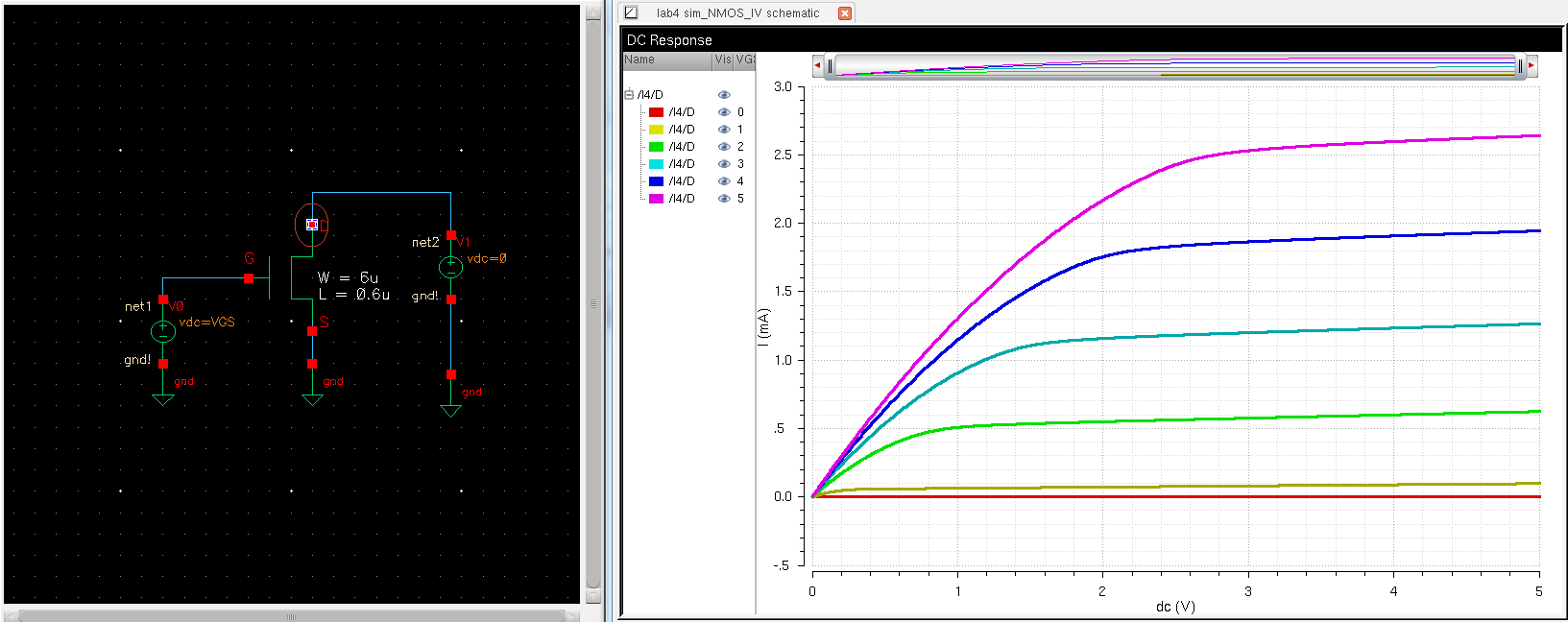
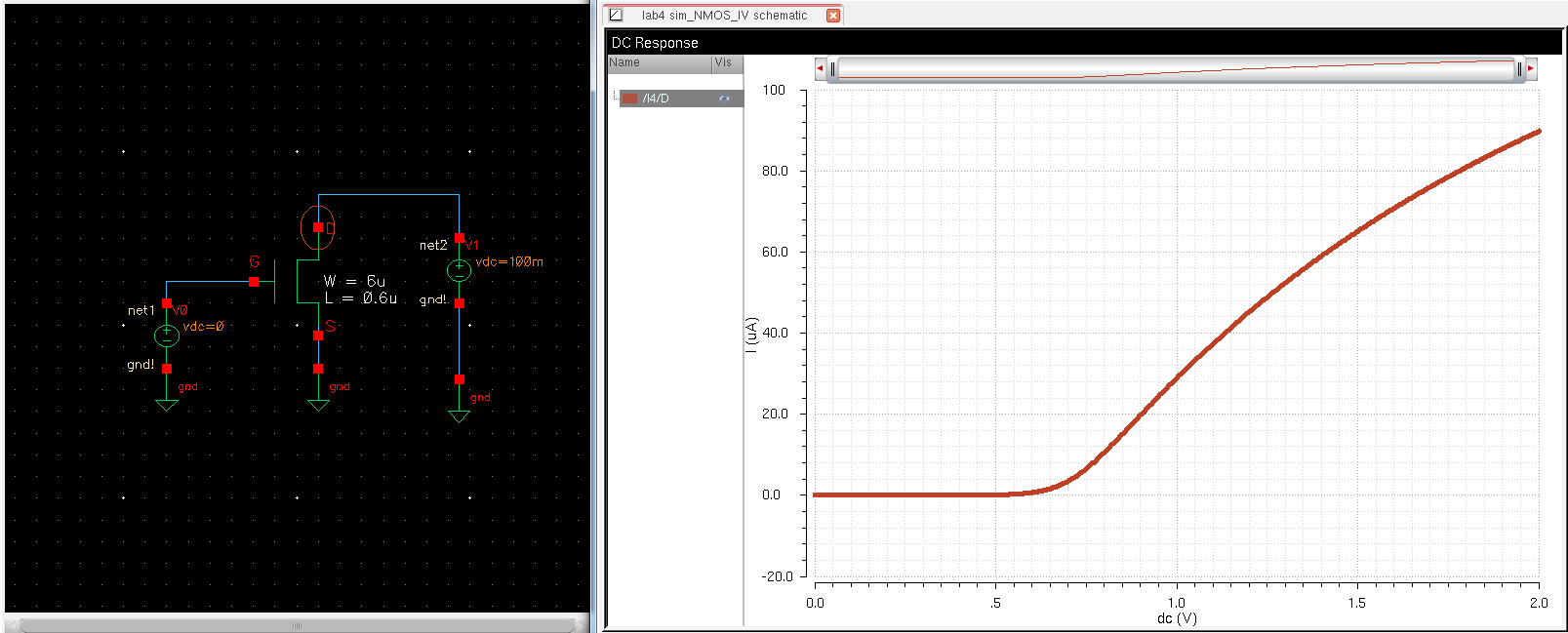
- Below
are
the simulations listed in the lab requirements. To simulate, variables
were used to step and sweep the needed voltages. Parametric analysis
was needed in the Analog Design Environment to generate the correct
curves. As one can see, the characteristic curves were generated to get
an idea how the devices operate in given conditions.
Exercise #2: Layout
a 6u/0.6u NMOS device and connect all 4 MOSFET terminals to probe pads
(which can be considerable smaller than bond pads [see MOSIS design
rules] and directly adjacent to the MOSFET (so the layout is
relatively small).
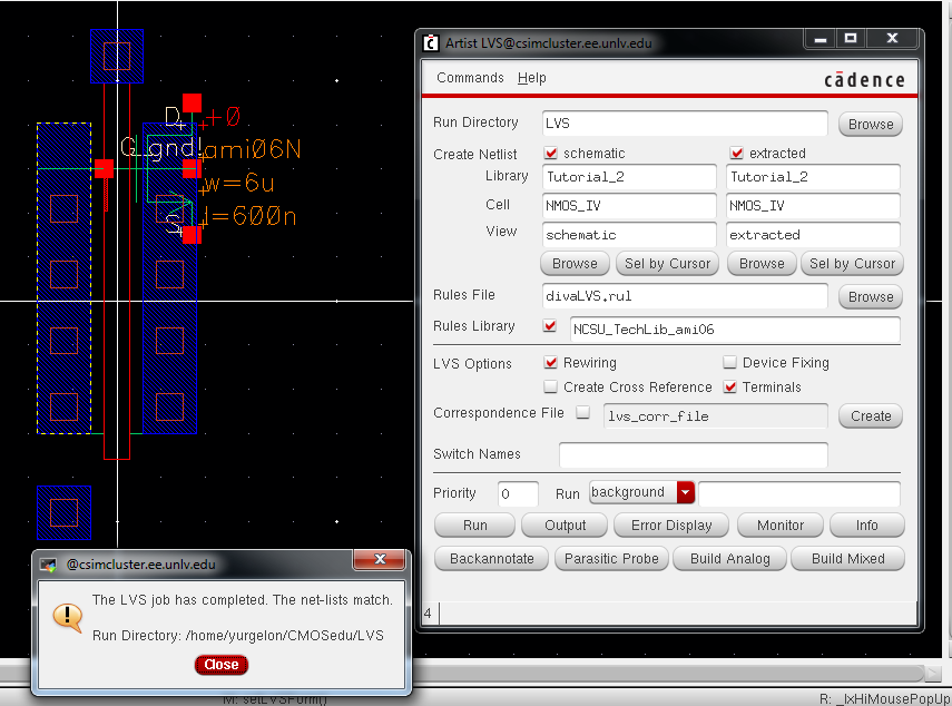
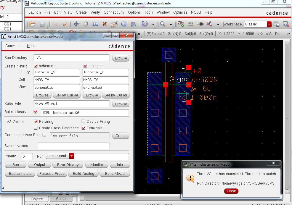
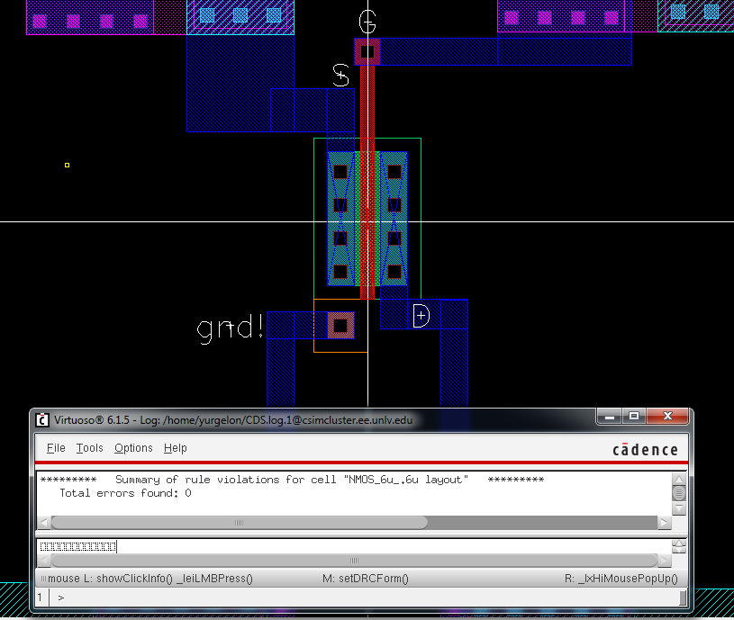
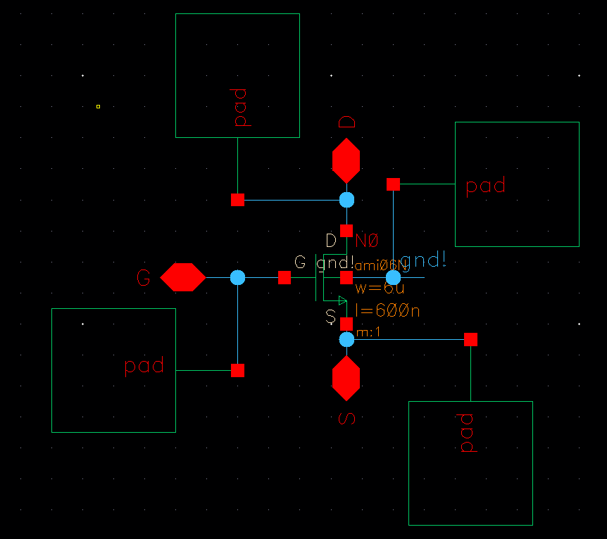
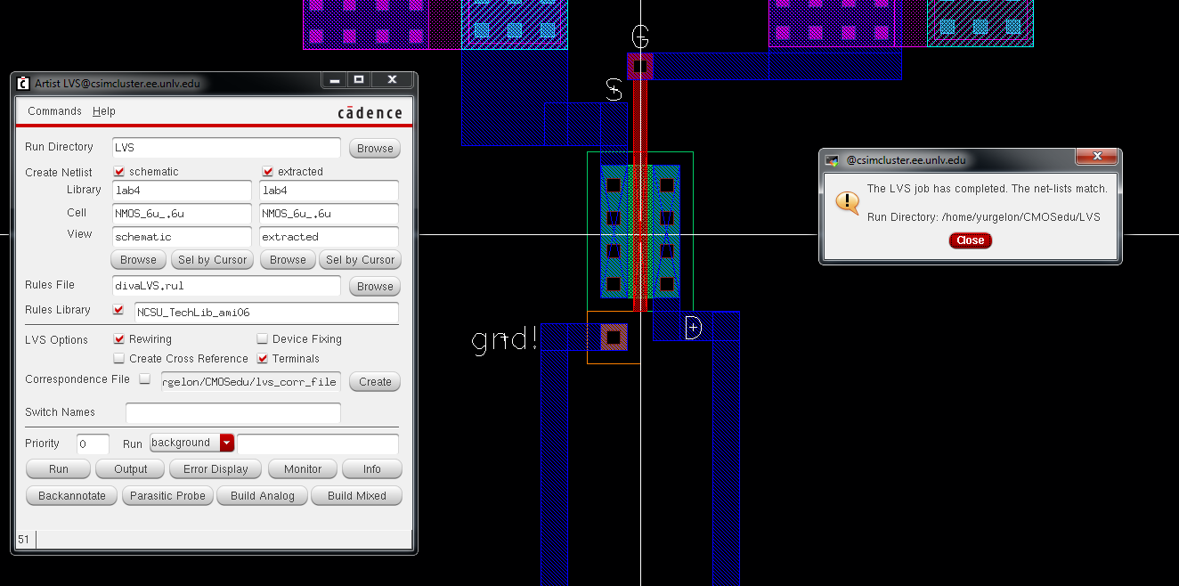
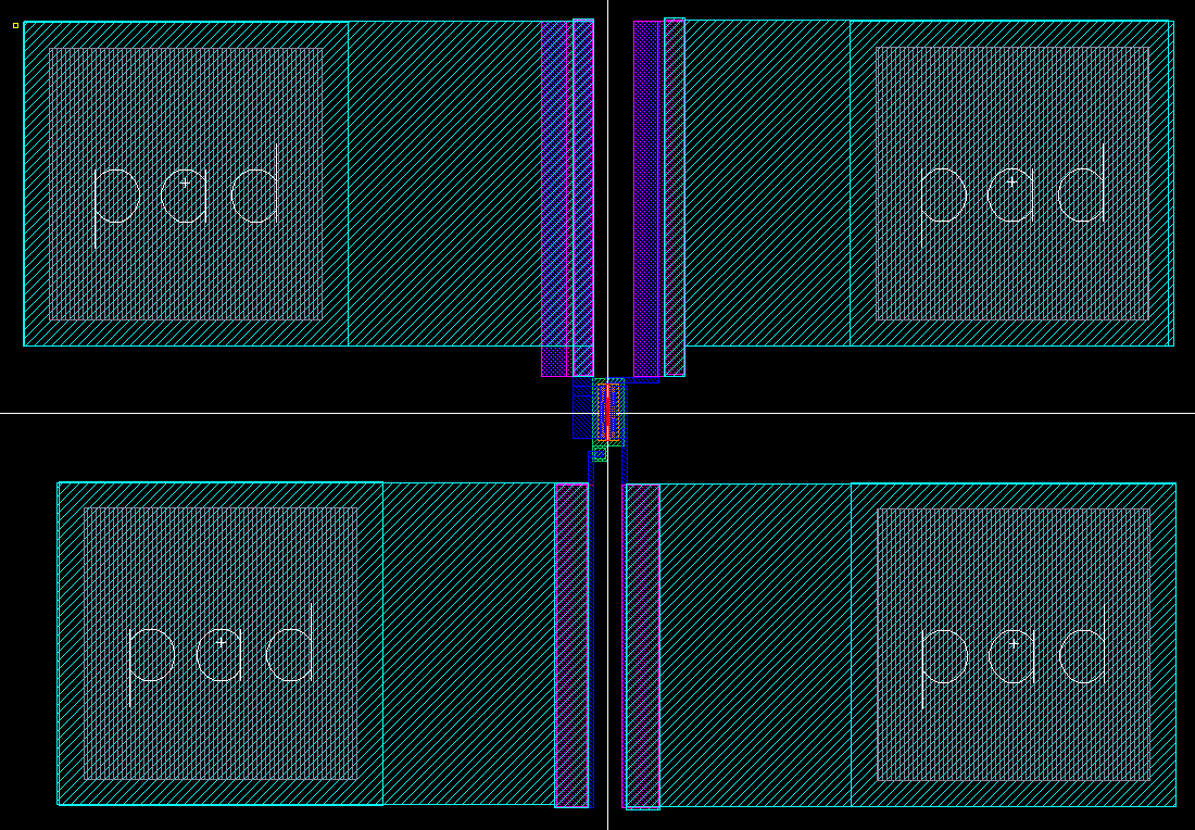
- Below
are the necessary pictures documenting the layout of the NMOS device.
Each terminal of the device was connected to a probe pad. A
corresponding schematic was created to create a one to one
correspondance between the schematic and the layout. No DRC errors were
found.
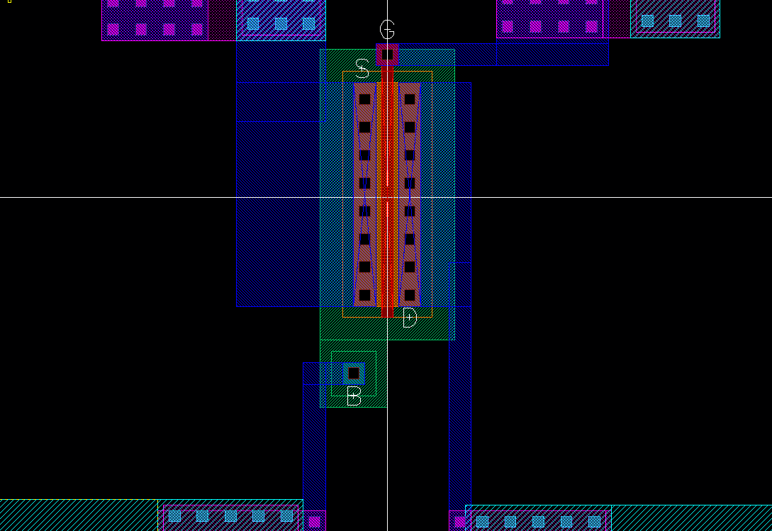
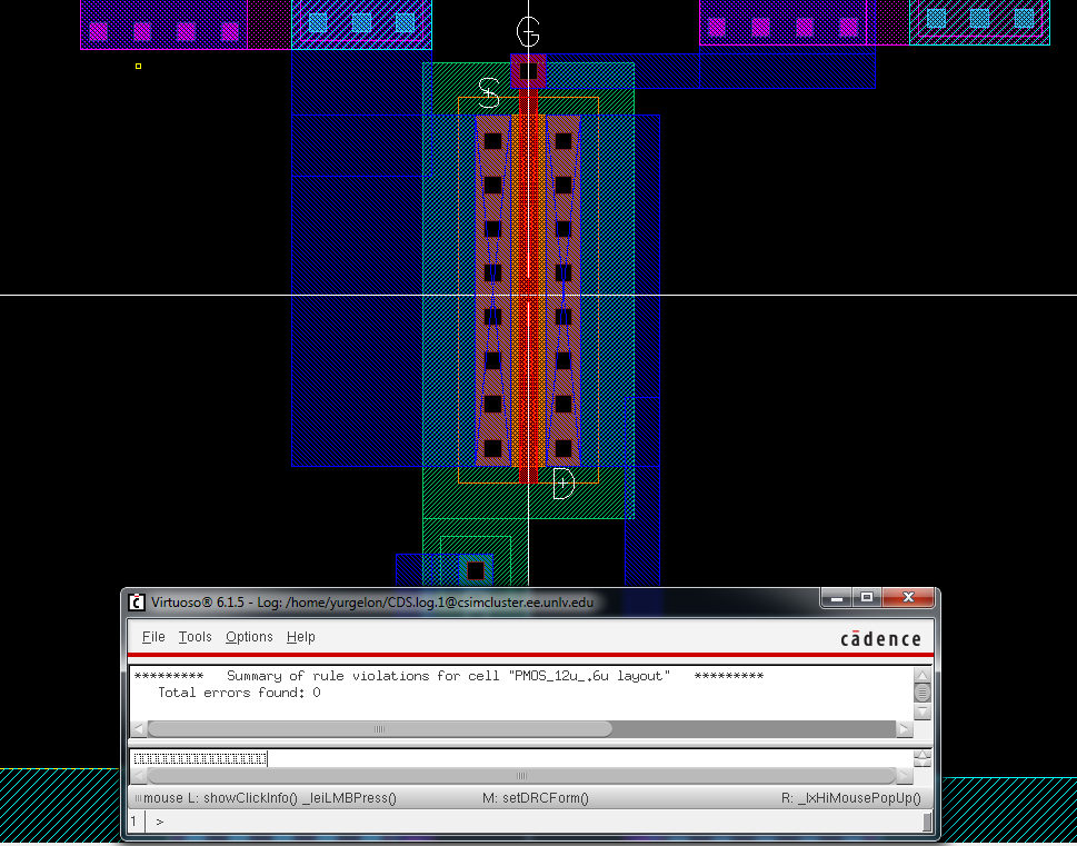
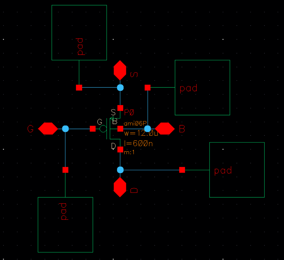
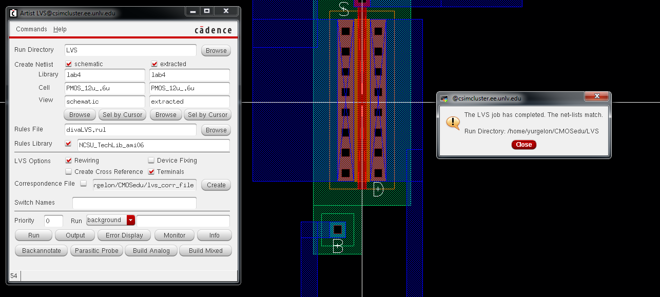
Exercise #3: Layout
a 6u/0.6u NMOS device and connect all 4 MOSFET terminals to probe pads
(which can be considerable smaller than bond pads [see MOSIS design
rules] and directly adjacent to the MOSFET (so the layout is
relatively small).
- Below are the necessary pictures documenting the layout of the PMOS device. Each terminal of the device was connected
to a probe pad. A corresponding schematic was created to create a one
to one correspondance between the schematic and the layout. No DRC
errors were found.
Return to EE 421L Labs