Lab 2: Design of a 10-bit Digital-to-Analog Converter (DAC) - EE 421L
Authored By: Joey Yurgelon
Email: yurgelon@unlv.nevada.edu
August 30, 2015
Pre-lab Work:
- Back-up all of your work from the lab and the course.
- Read through this entire lab write-up before doing the pre-lab
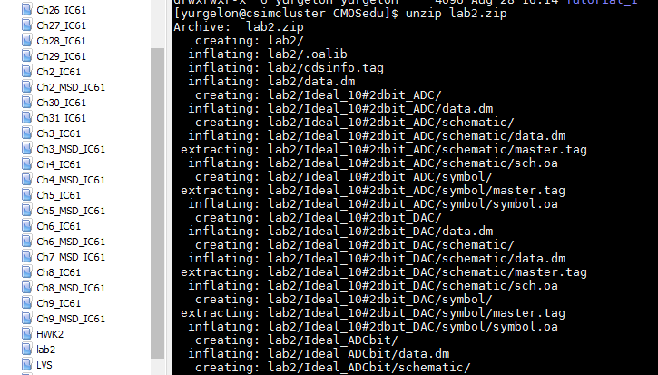
- Download lab2.zip to your desktop.
- This
archive contains a simulation example using an ideal 10-bit
Analog-to-Digital Converter (ADC) and Digital-to-Analog Converter
(DAC).
- Upload this zip file to the design directory on the server that you are running Cadence from, e.g., Tutorial_1, CMOSedu, etc.
- Note that it's assumed you are using the NCSU Cadence Design Kits.
- Unzip this directory and add, to your cds.lib in the design directory, the following statement (assuming the design directory is CMOSedu):
- DEFINE lab2 $HOME/CMOSedu/lab2
- Start Cadence from the design directory.
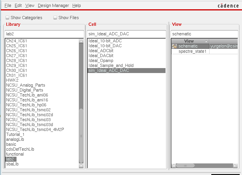
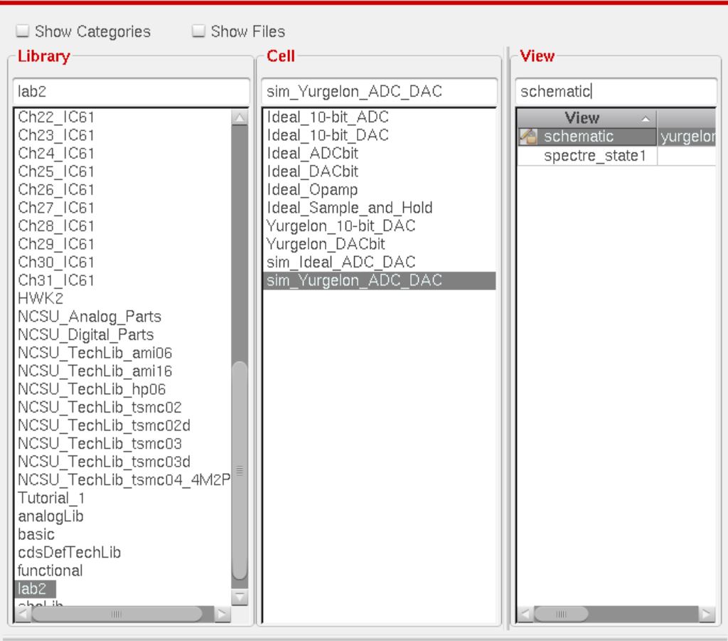
- Use the Library Manager and navigate to the lab2 Library as seen below.
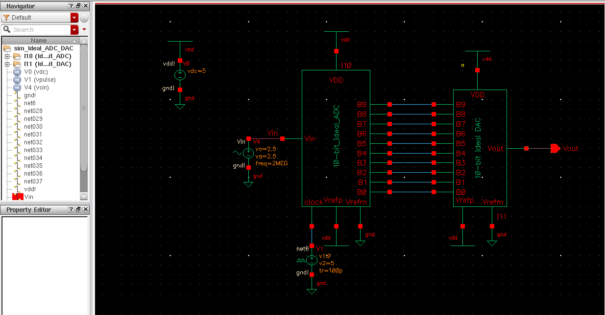
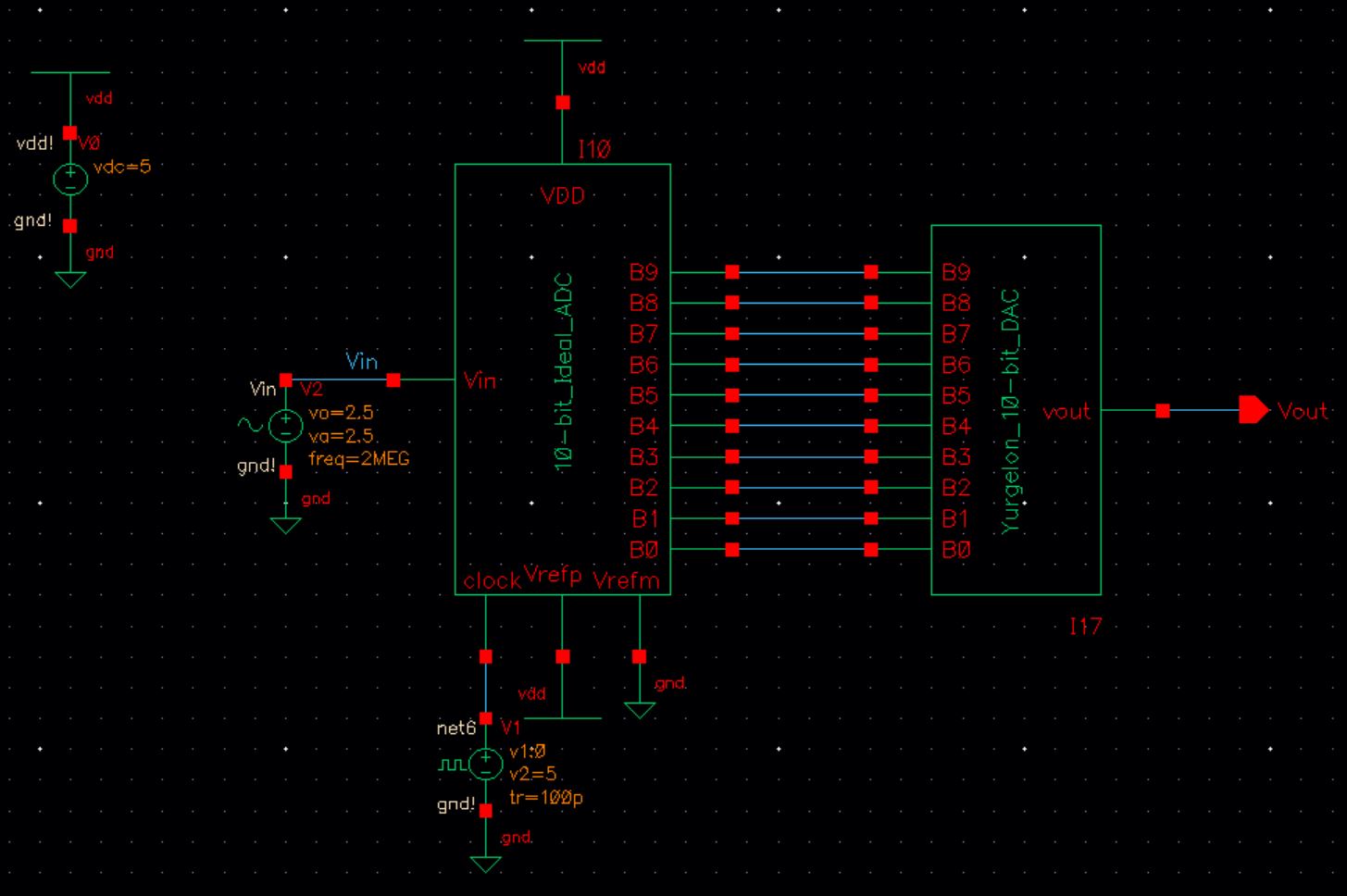
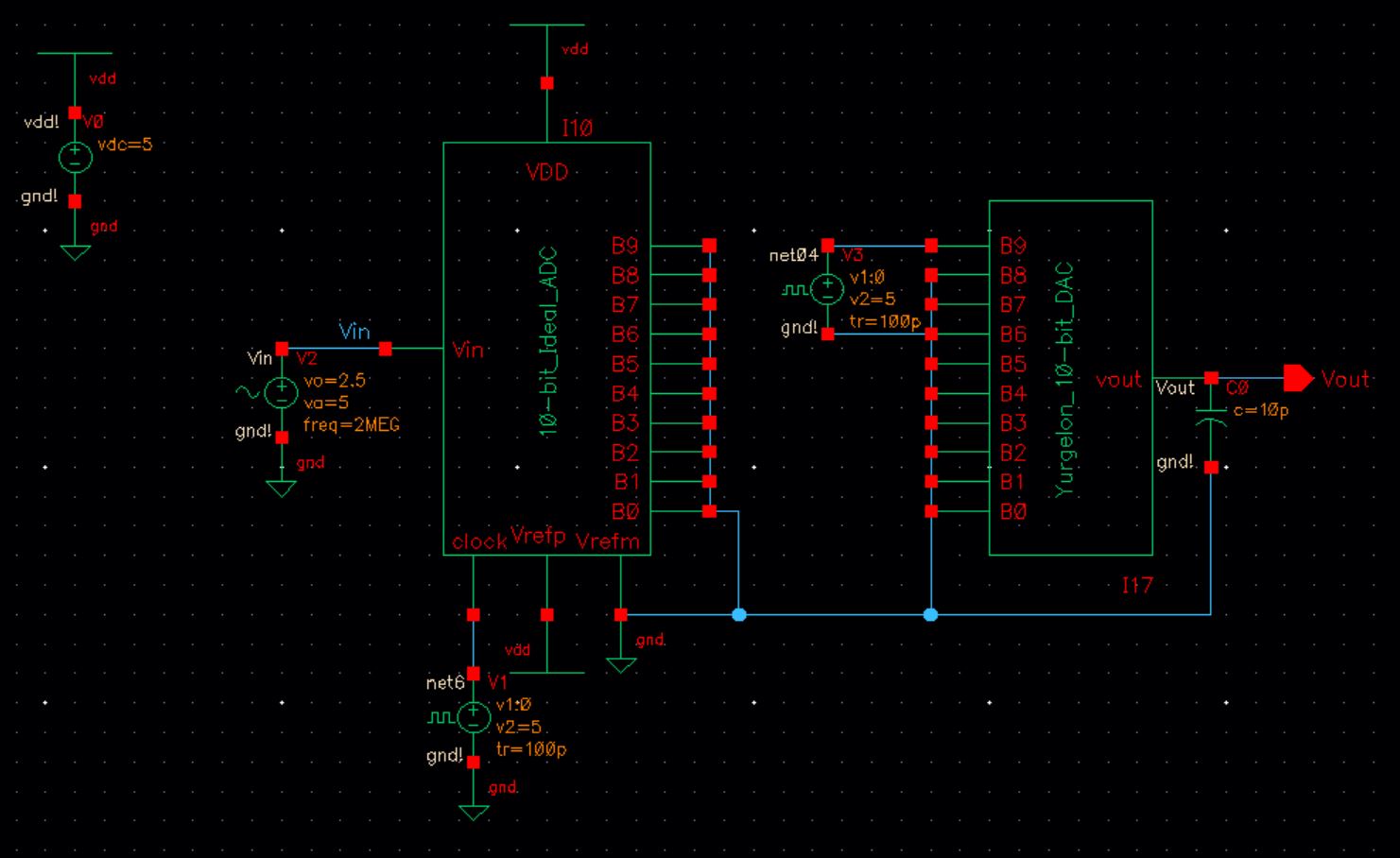
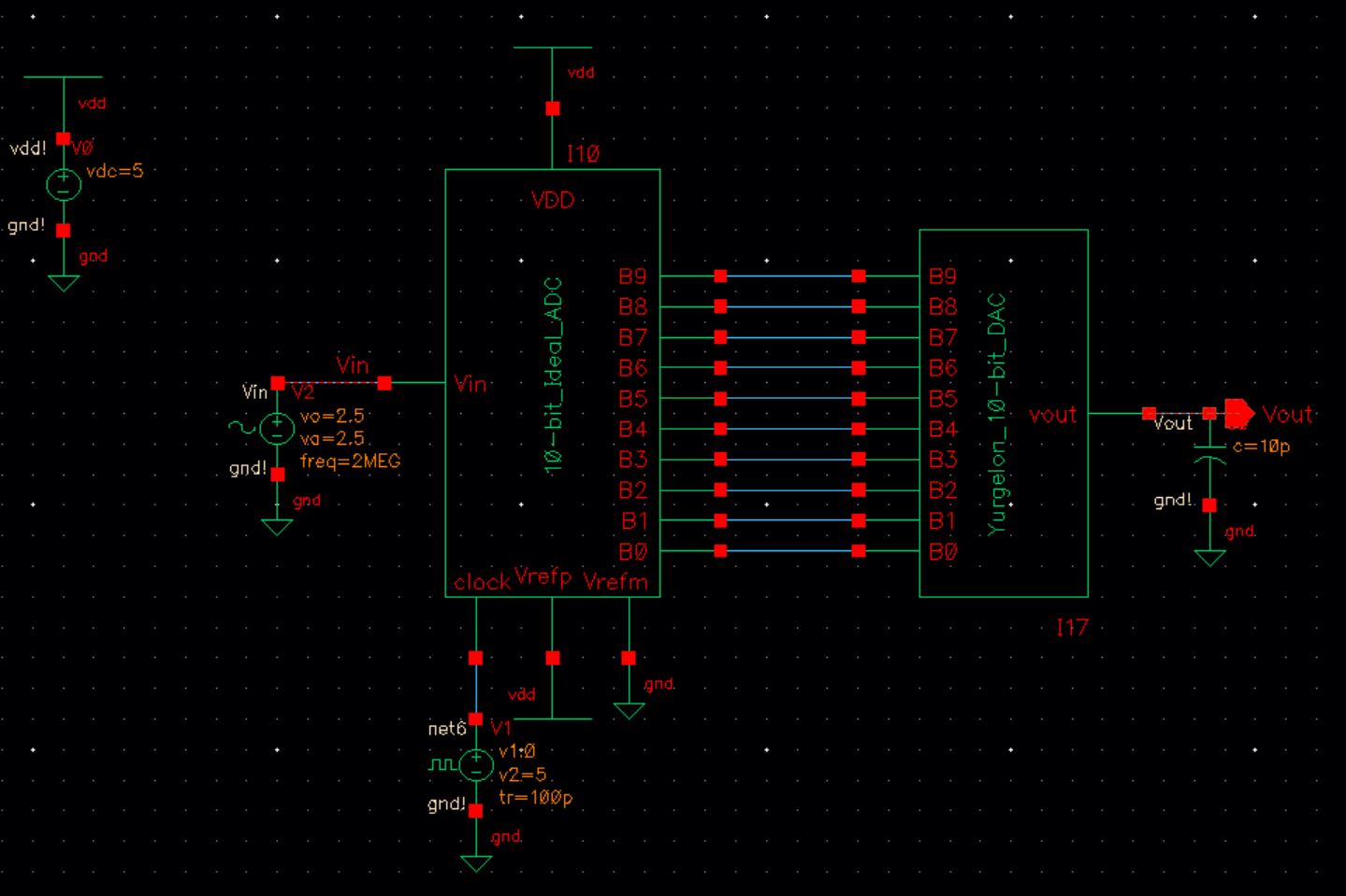
- Open the schematic view of the cell sim_Ideal_ADC_DAC.
- This cell contains the ideal 10-bit ADC and DAC as seen below in the second image.
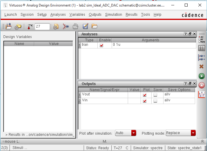
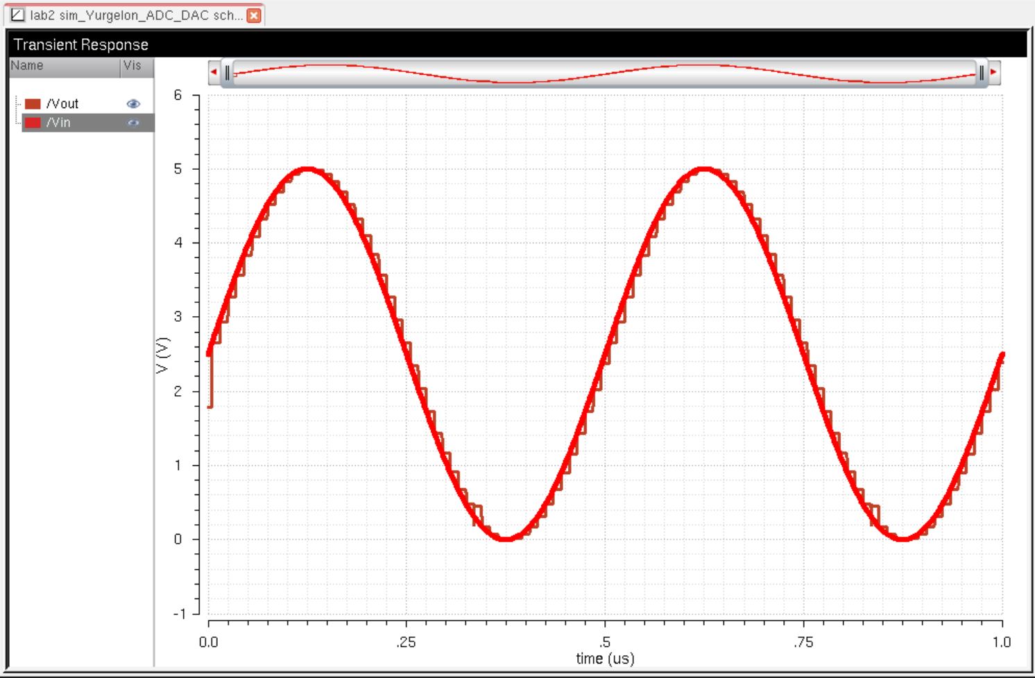
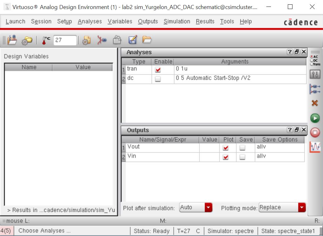
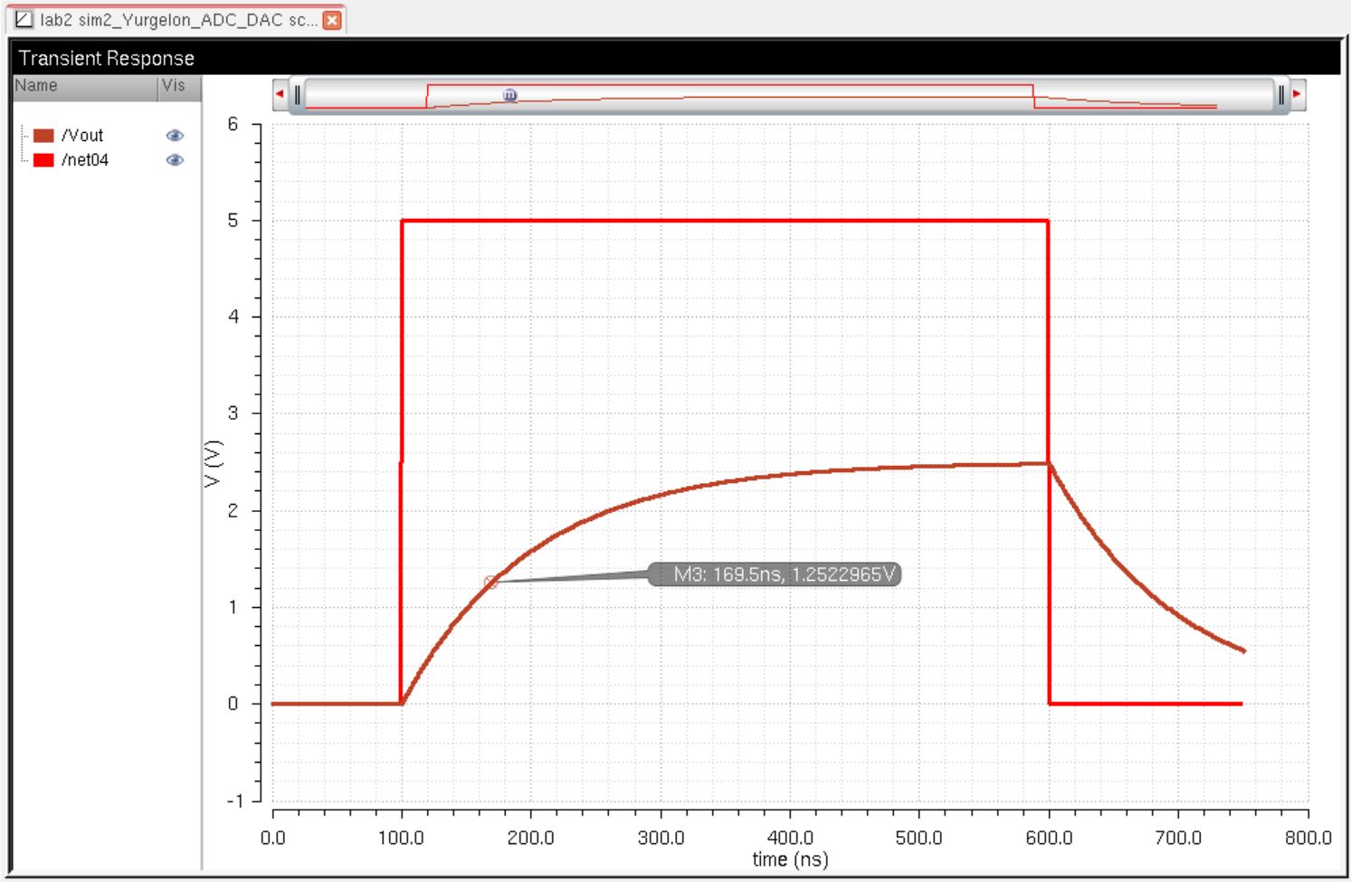
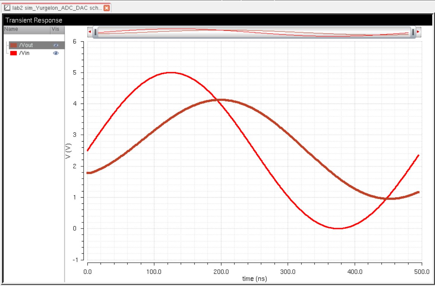
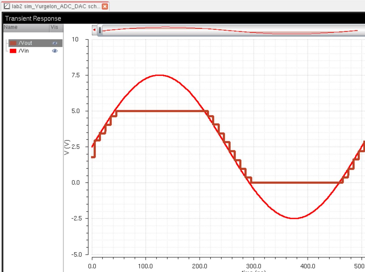
- Run
the simulation (Launch the ADE, Session -> Load State -> Cellview
-> OK, press the green start button) to get the following.
- Make sure you understand how to change the background color, line thickness, and type of line (e.g. solid, dashed, etc.)
- Prior to coming to lab make sure you understand how the input voltage, Vin, is related to B[9:0] and Vout (the quiz may ask a question about this).
- In
your lab report: 1) provide narrative of the steps seen above, 2)
provide, and discuss, simulation results different from the above to
illustrate your understanding of the ADC and DAC, 3) explain how you
determine the least significant bit (LSB, the minumum voltage change on the ADC's input to see a change in the digital code B[9:0]) of the converter. Use simulations to support your understanding.
- Backup your webpages and design diretory.
Exercise #1: Provide a narrative of the steps seen above.
- After
downloading the lab2.zip file above, I was able to easily navigate to
the CMOSedu design directory and upload it through the Xterm interface
(Discussed in Tutorial 1). I was then able to use the command "unzip
lab2.zip" to release all of the zipped files. Cadence then needs to
know where to look to find the project files for the DAC/ADC
simulations, as such, "DEFINE lab2 $HOME/CMOSedu/lab2" was added to the bottom of the "cds.lib" file.
- After
following thtose steps, one can then pull up the project via the
library manager, and then open the schematic file. To simulate, we
navigate to the "Launch" tab, and click on "ADE L." This will birng up
the environment for setting up simulations. Since one has already been
created, we can load it via the "Session" tab and loading in a save
state with the cell view. After clicking the green button with the
pre-configured settings, we can see our results.
- Photos highlighting milestones in the process can be seen below.
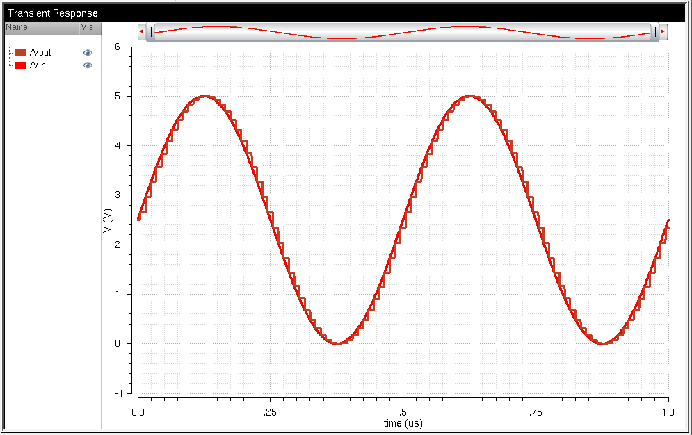
Exercise #2: Provide, and discuss, simulation results different from the above to illustrate your understanding of the ADC and DAC
- The
DAC works by attaching a voltage weight to a digital input bit. Due to
its linearity, then can then sum all of the voltage weights together to
produce an output represented weighted by the supply voltage and the
number of bits. The quality of the DAC depends on how well the
resistors are matched as well as its bit depth in relation to the
supply voltage. For example, a 10-bit DAC's LSB sits around at 4 mV
with a 5V VDD, but increases to 9 mV at 10V VDD. This demonstrates that
the bit depth is the primary factor in the accuracy of the device with
a large input envelope.
Exercise #3: Explain how you determine the least significant bit (LSB, the minumum voltage change on the ADC's input to see a change in the digital code B[9:0]) of the converter. Use simulations to support your understanding.
- To
determine the LSB of the DAC, we first need to see the amount of
birnary words that can be covered. With ten inputs, each with two
states (0 or 1), we can calculate this to be 2^N where N = 10 or 1024
binary combinations. The supply voltage can then be divided by this
number to determine the LSB of the device. 1 LSB = 5V/1024 = 4.883 mV.
Lab Description:
- Students
will learn how build the schematic and symbol for the 10-Bit DAC.
Lab Requirements:
- The design of a 10-bit DAC using an n-well R of 10k
- The 2R resistor should be implement with two separate 10k resistors in series
- After you've designed and drafted your schematic check and save it
- How to determine the output resistance of the DAC (answer: R) by combining resistors in parallel and series
- Delay, driving a load
- Ground
all DAC inputs except B9. Connect B9 to a pulse source (0 to VDD) and
show, and predict using 0.7RC, the delay the DAC has driving a 10 pF
load
- Verify the simulation results match your hand calculations
- How
to create a symbol view for your design with the exact same footprint
as the Ideal_10-bit_DAC symbol view (hint: use Copy before you
start drafting your design, e.g. Copy the cell Ideal_10-bit_DAC to
Mydesign_10-bit_DAC and then simply edit the schematic view!)
- See Tutorial 1 for additional help
- Note that your design won't use VDD, Verfp, or Vrefm so you can delete those pins on your design's DAC symbol view
- Simulations to verify your design functions correctly.
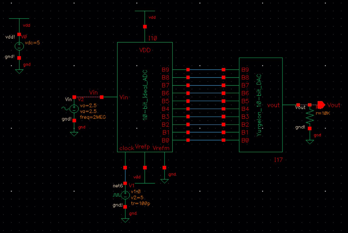
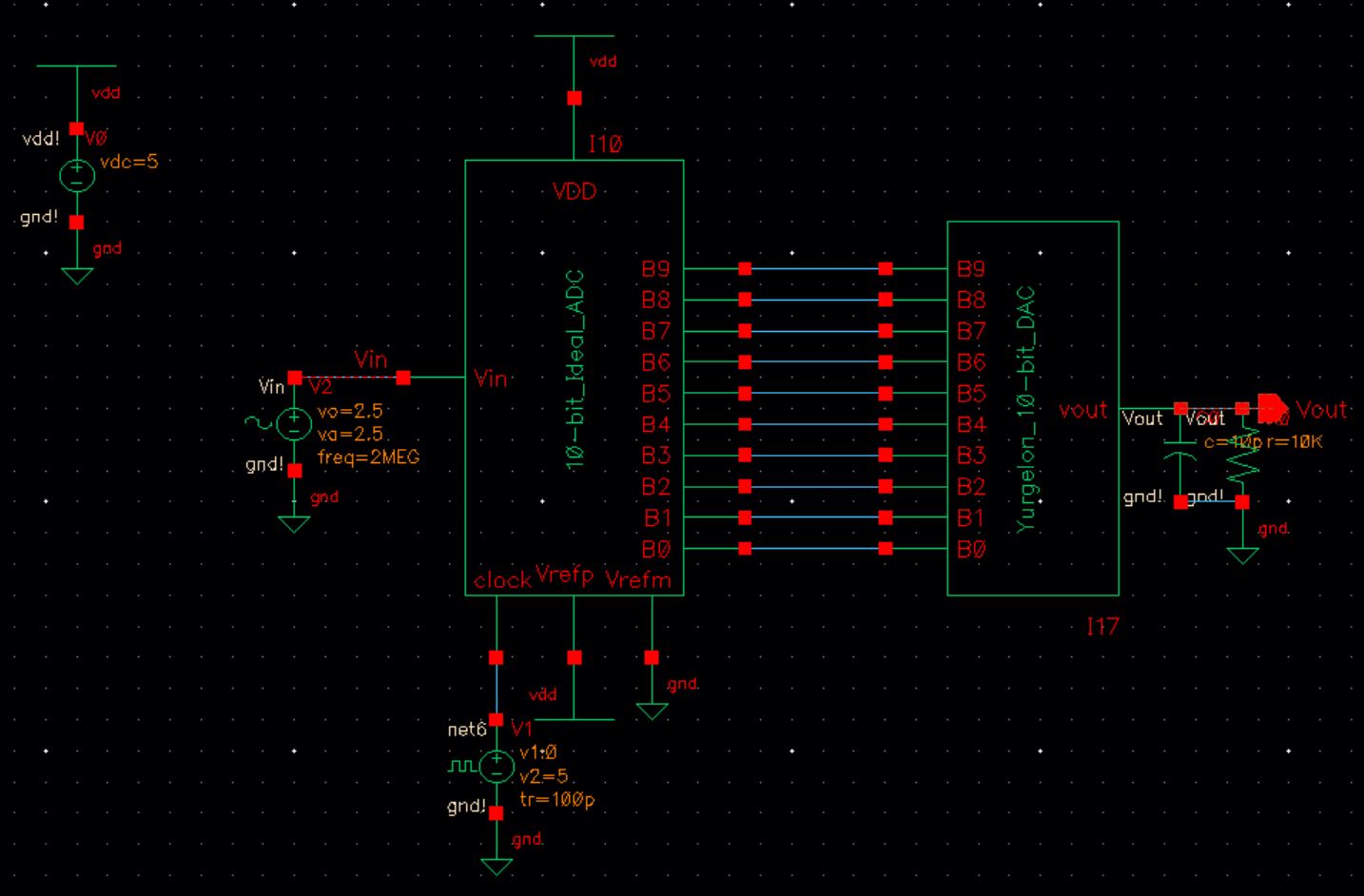
- Copy the schematic cell view sim_Ideal_ADC_DAC to a cell sim2_Ideal_ADC_DAC and replace the ideal DAC with the one you just designed
- Use the sim2_Ideal_ADC_DAC to illustrate that your design works as expected.
- Show what happens if the DAC you designed drives a load (both R, C, and R/C)
- Explain what happens if the DAC drives a 10k load?
- In a real circuit the switches seen above (the outputs of the ADC) are implemented with transistors (MOSFETs).
- Discuss what happens if the resistance of the switches isn't small compared to R.
- If you have simulation convergence problems you can force the simulation to converge by going to, in the ADE, Simulation -> Options -> Analog
- Set the values as seen below
- relative tolerance, reltol, of 10% (= 1e-1)
- voltage absolute tolerance, vabstol, of 100 mV (= 1e-1)
- current absolute tolerance, iabstol, of 1 mA (= 1e-3)
- The accuracy of the simulation will, obviously, be degraded
Experimental Results:
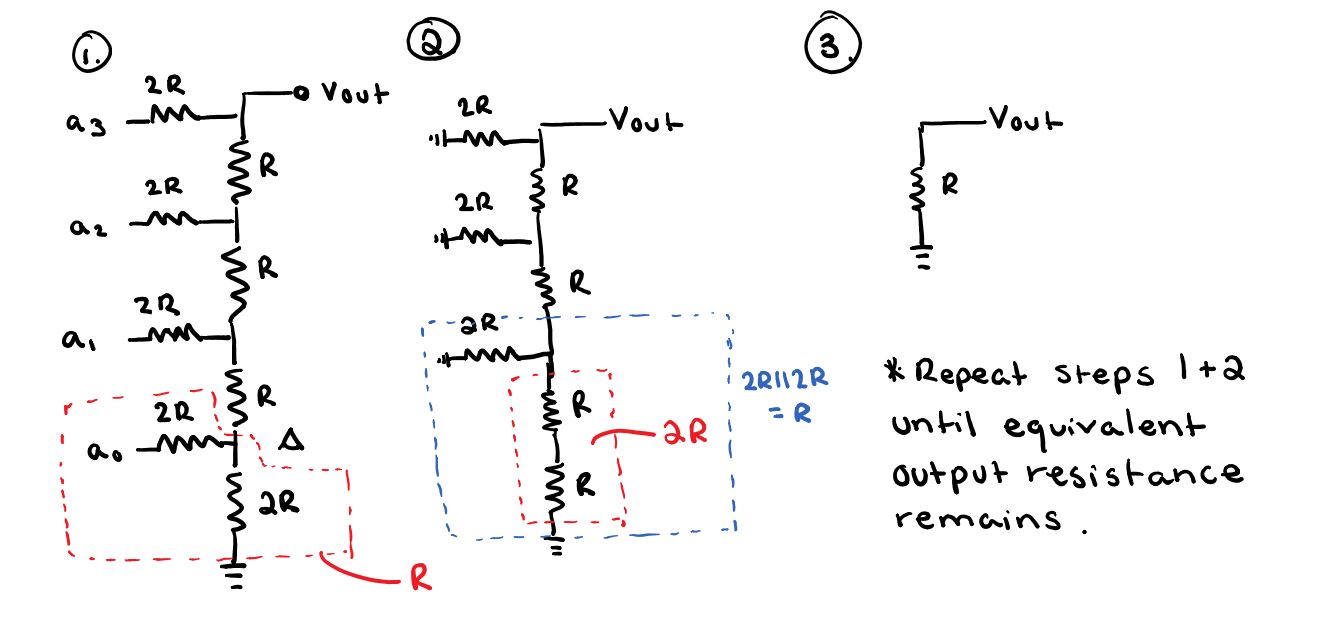
Exercise #1: Show how to determine the output resistance of the DAC (answer: R) by combining resistors in parallel and series.
- This
calculation is very easy to do by hand, and is vital to understanding
the output one might obtain when connecting any sort of lead to the
circuit. To start, we want to look at the least significant bit on the
DAC, and assume all bit connections are shorted to ground. By taking
note of this, we can start to see that we have two 2R resistors
connected in parallel, and by finding the equivalent resistance, we
obtain R. This equivalent resistance can be summed with the resistor
connecting the most significant bit with the second most significant
bit. By doing so, we obtain a resistance of 2R once again. This
resistance can then be connected in parallel with the other 2R, and so
on. After all of the ladders have been taken care of, we should have an
output resistance of R. The results of this can be seen below.
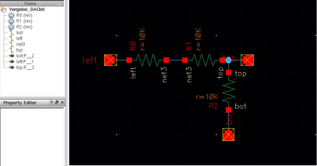
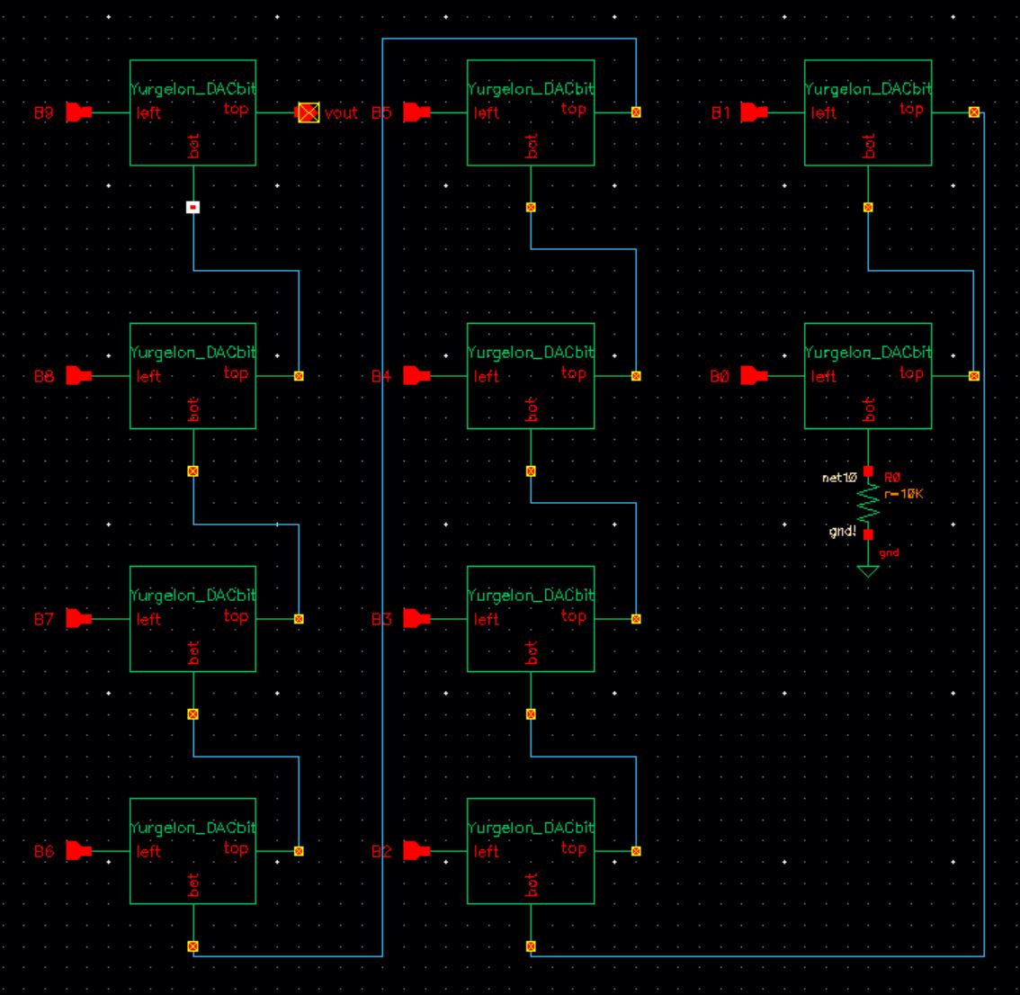
Exercise #2: The design of a 10-bit DAC using an n-well R of 10k.
- The
design of the 10-bit DAC was straightforward. I started out by copying
over as much as I could from the pre-lab files, and then altered them
as needed. To start, I created a single 'DAC-Bit' which would serve as
the basic building block to the DAC. I would use this 'DAC-bit' to
produce the larger 10-bit DAC by stringing 10 of them together. After
connecting them as needed, a symbol was created so that the design may
be tested with the pre-lab configuration. Details of such work can be
seen in the pictures below.
Exercise #3: Ground
all DAC inputs except B9. Connect B9 to a pulse source (0 to VDD) and
show, and predict using 0.7RC, the delay the DAC has driving a 10 pF
load.
- After
setting up the device in the desired configuration, we can easily go
through the calculations needed to predict the delay time with a 10 pF
load. As mentioned in Exercise #1 above, the output resistance of the
ladder DAC is R no matter how many bits exist. Knowing this, we can
determine the R in our equation to be 10 k Ohms. The time delay then is
as follows: Time Delay = 0.7*10K*10p = 70 nS. This was comparable to the simulated result.
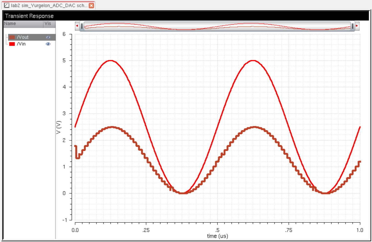
Exercise #4:Verify
the design works by simulation. Show the output when the DAC drives a
load (R, C, and R/C). Explain what happens if the DAC drives a 10k load?
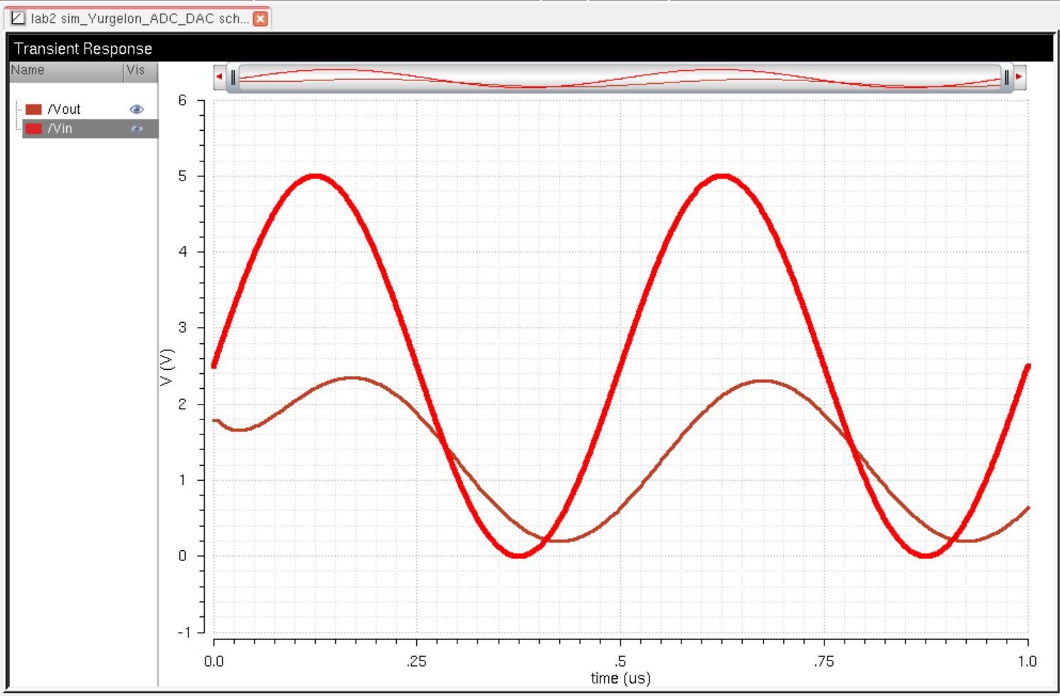
- Since
the output resistance of the DAC is 10k Ohms, connecting the device to
a 10k Ohm load will result in a sinusoid with half the ouutput
amplitude as the input. This is due to the voltage divider effect that
will persist. As one can see below, the various loads produces various
alterations to the input. On the left side of the table below, one will
find the circuit used to simulate the output on the right hand side. It
is clear that both types of loads cause a reduction in the amplitude,
but only when the capacitor is set is there a phase shift on the
output.
- In a real circuit the switches seen above (the outputs of the ADC) are implemented with transistors (MOSFETs). Discuss what happens if the resistance of the switches isn't small compared to R?
- If
the resistance of the switches is not small compared to R, there will
be significant loading effects on the output. Only when the output has
a significantly high resistance do we see a complete reproduction of
the input signal. In an ideal voltage meter, the input resistance is
infinite to prevent altering the signal upon measurement.
Return to EE 421L Labs