Project - EE 421L
Vrigiank@unlv.nevada.edu
Kirk Vrigian
11/6/15
Lab
description
The final project includes the schematics and simulations of the following circuits:
- Design of an 8-bit resettable (input "clear") up/down counter
- The outputs of your counter should be buffered before connecting to a pad
- A 31-stage ring oscillator with a buffer for driving a 20 pF off-chip load
- NAND and NOR gates using 6/0.6 NMOSs and PMOSs
- An inverter made with a 6/0.6 NMOS and a 12/0.6 PMOS
- Transistors,
both PMOS and NMOS, measuring 6u/0.6u where all 4 terminals of each
device are connected to bond pads (7 pads + common gnd pad)
- Note
that only one pad is need for the common gnd pad. This pad is used to
ground the p-substrate and provide ground to each test circuit
- Using
the 25k resistor laid out below and a 10k resistor implement a voltage
divider (need only 1 more pad above the ones used for the 25k
resistor)
- A 25k resistor implemented using the n-well (connect between 2 pads but we also need a common gnd pad)
Lab procedure:
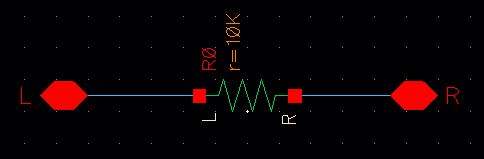
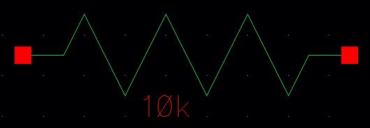
25K Resistor
Below are the schematic, symbol, simulation circuit & corresponding simulation results.
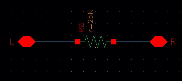
25K Resistor schematic
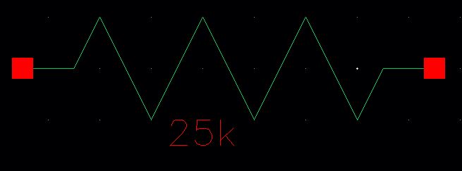
25K Resistor symbol (using create from cellview)
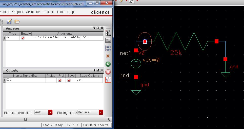
Simulation Circuit (along with simulation parameters).
By sweeping the voltage source (using dc sweep analysis) from 0-5 volts
we can verify that the 25k resistor is working by comparing the linear
relationship V=IR
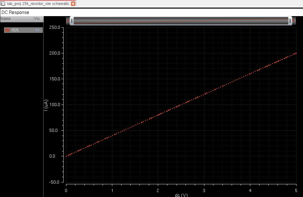
Simulation Results
The results support our linear relationship of a 25k resistor. At 5V we get an I of 200uA.
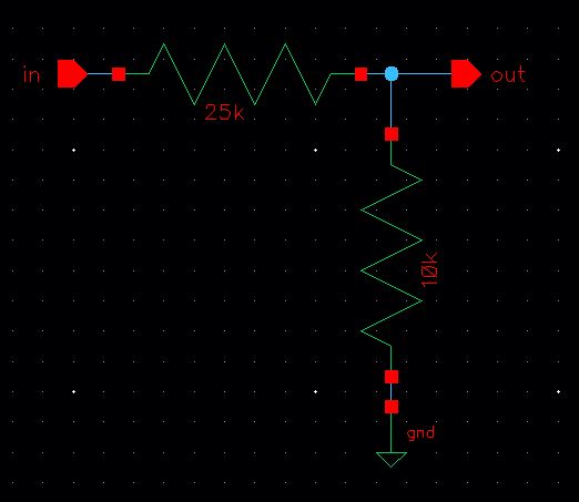
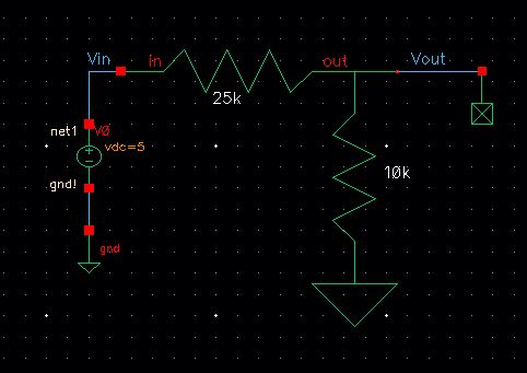
Voltage Divider:
Next,
create a voltage divider utilizing a 25k resistor followed by a 10k
resistor. Like before, create a 10k resistor & corresponding symbol.
Schematic
Symbol
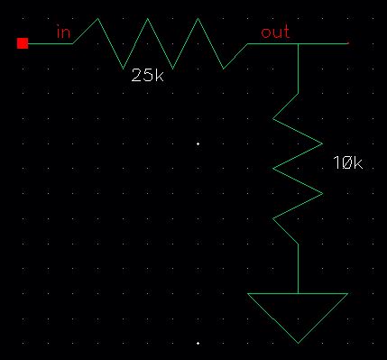
Now to create the voltage divider schematic, symbol & finally the test schematic utilizing the voltage divider symbol.
Schematic for voltage divider
Corresponding voltage divider symbol
Simulation schematic
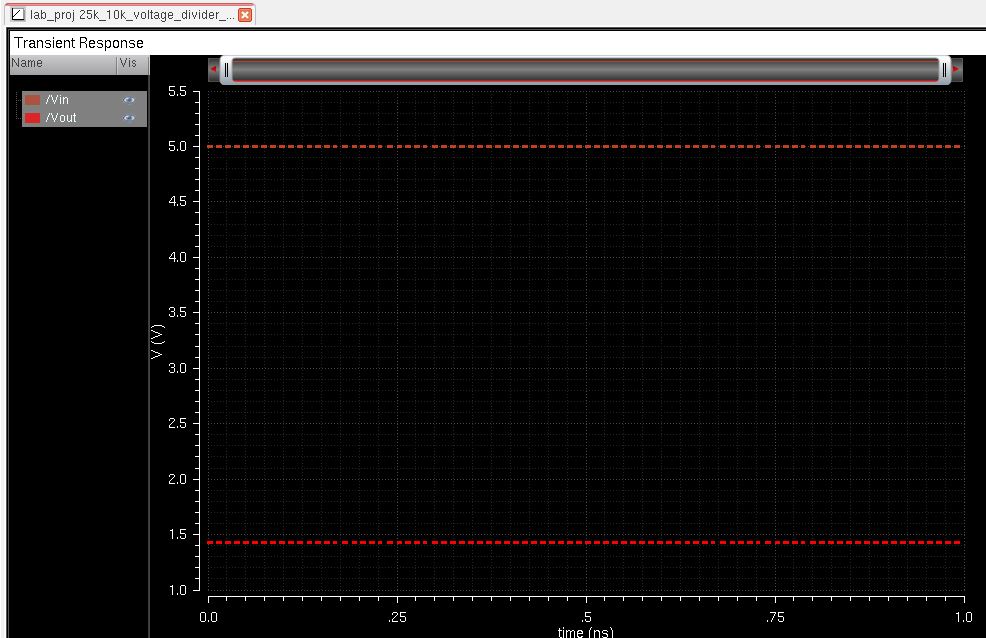
Simulation results (transient response of 1 nano).
Using an input of 5V, the expected output is
5*(10K)/(10K+25K) = 1.429V. The simulation confirms the voltage divider is working properly.
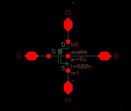
NMOS Transistor:
Below is the schematic, symbol & IV characteristic curves for a 6u/.6u NMOS transistor.
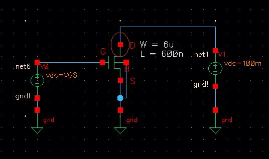
NMOS schematic
Simulation circuit using symbol (created from cellview)
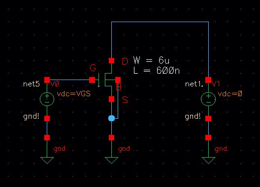
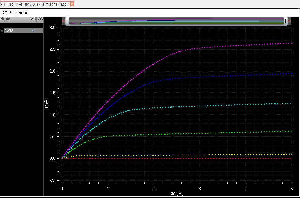
ID vs. VDS (sweeping VGS from 0-5 & VDS from 0-5 using a parametric analysis)
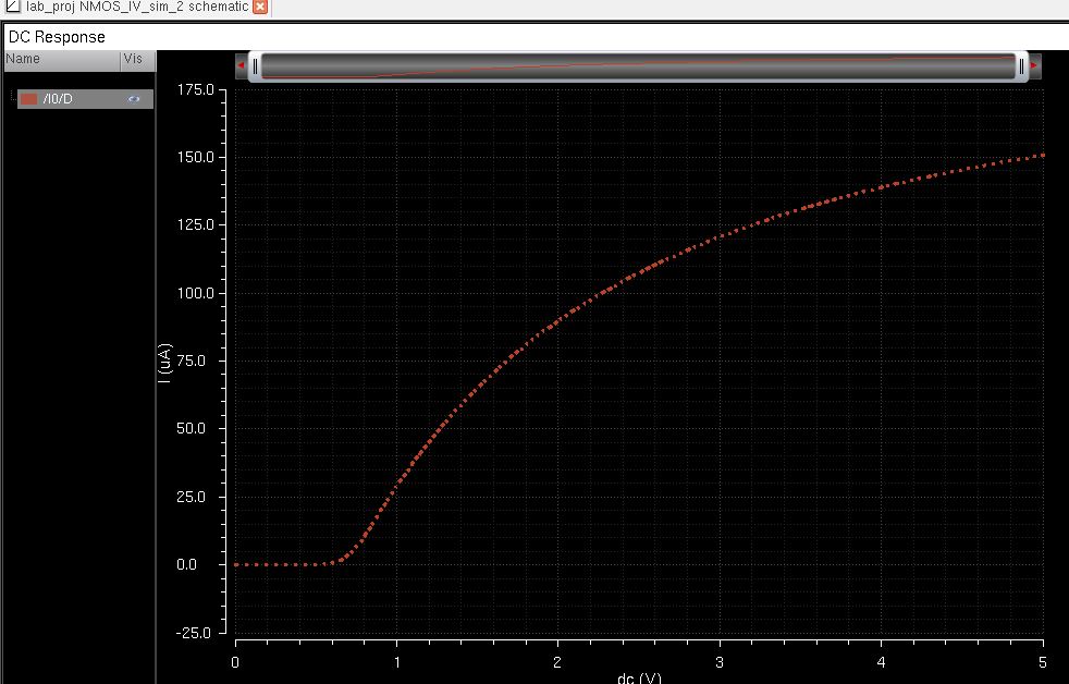
2nd simulation schematic for the same NMOS
This time it's ID vs. VGS and leaving VDS at 100mV.
Now for the PMOS transistor
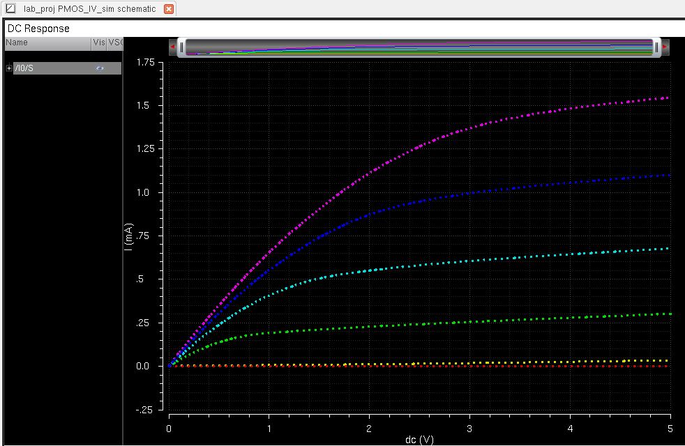
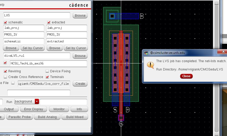
Below is the schematic, symbol along with IV characteristic curves for a 6u/.6u PMOS transistor.
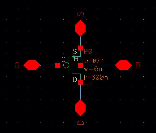
PMOS_IV Schematic
PMOS_IV simulation schematic using corresponding symbol
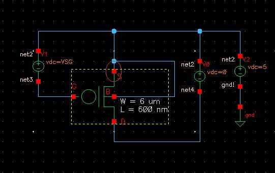
Again, using this schematic and using parametric analysis, one can generate ID vs. VSD by stepping VSG
2nd PMOS_IV simulation schematic
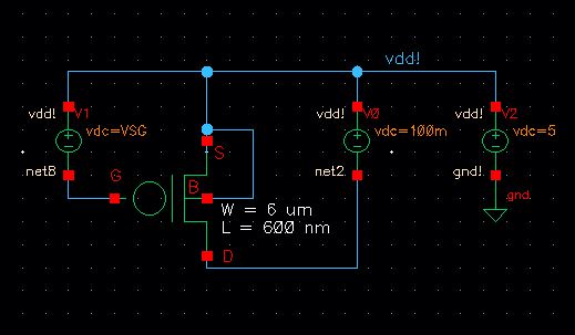
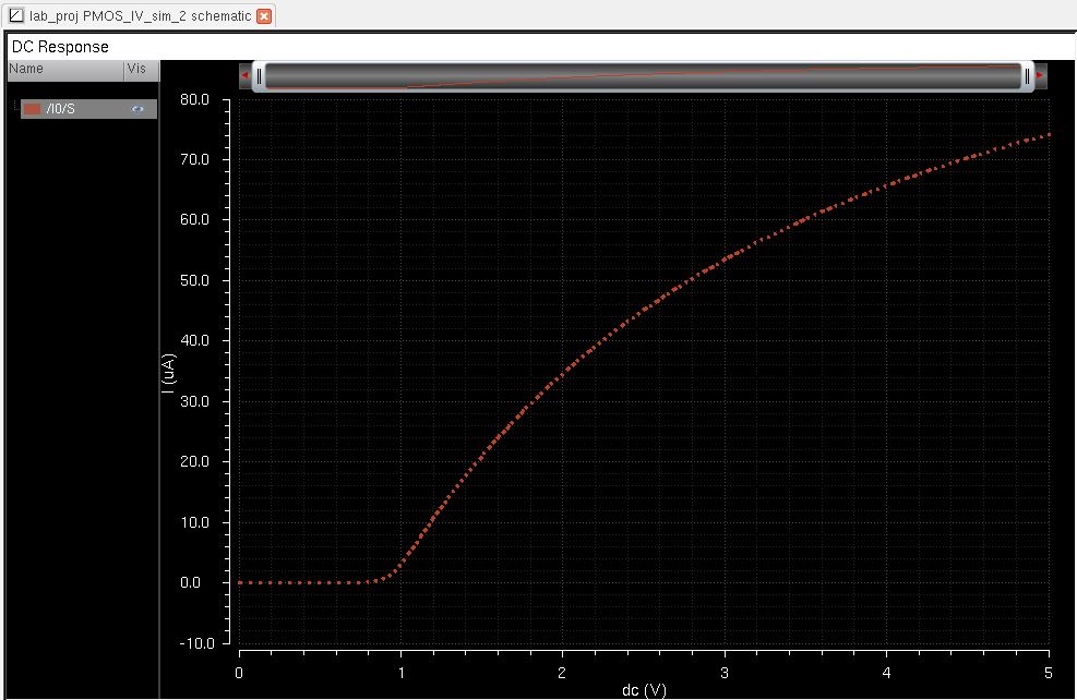
ID vs. VSG (using a vds of 100m & sweeping vsg from 0-5V)
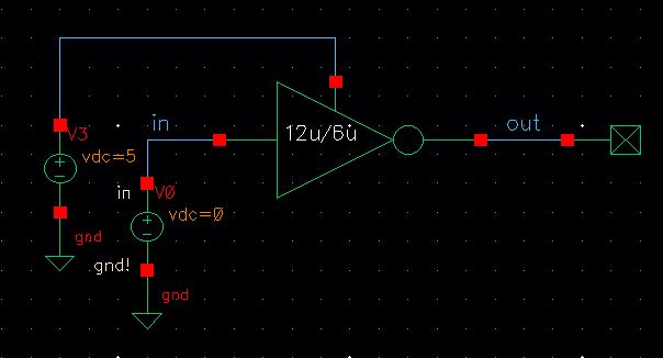
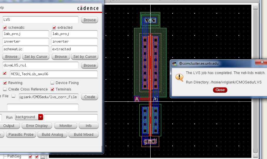
Inverter with 6u/.6u NMOS & 12u/.6u PMOS
Below is the schematic & simulation for the 12u/6u inverter.
Schematic of 12u/6u inverter
Simulation schematic of 12u/6u inverter (using symbol created from cellview)
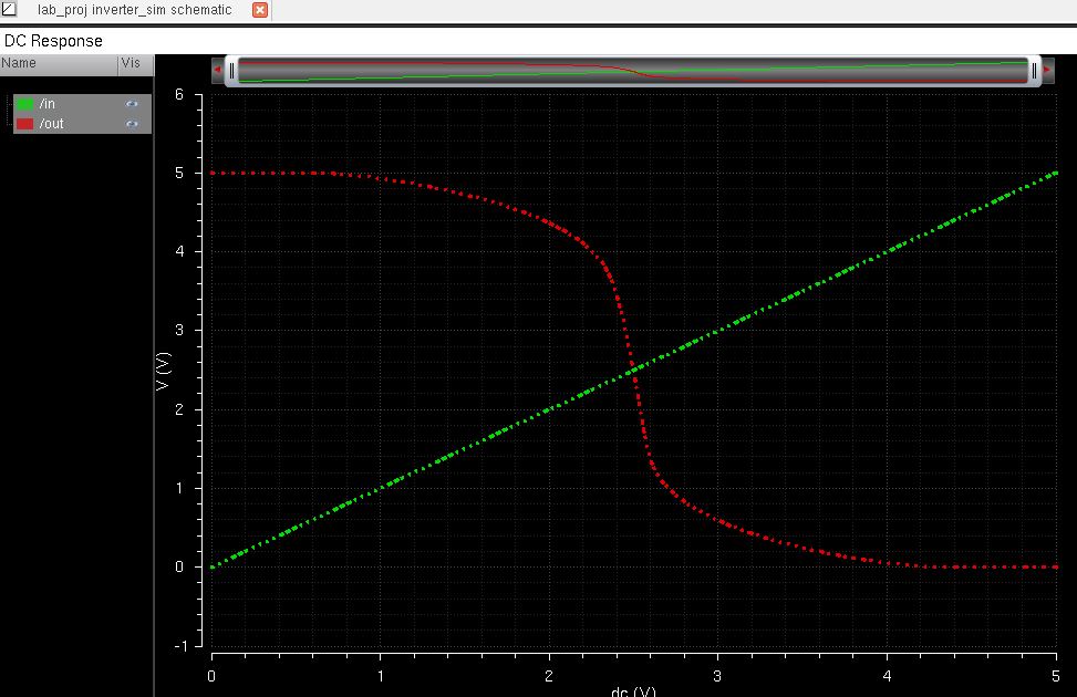
Doing a dc sweep from 0-5V of IN will result in the following results, showing that our inverter is working properly. The point the at which /in & /out instersect is our VSP.
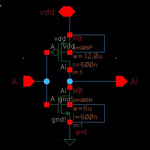
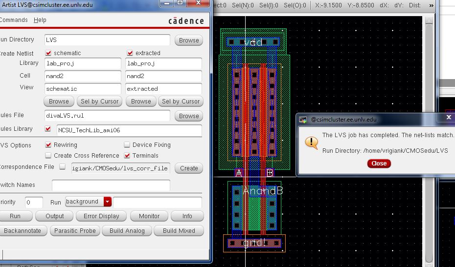
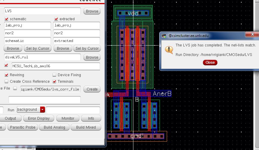
NAND/NOR gate utilizing 6u/.6u transistors
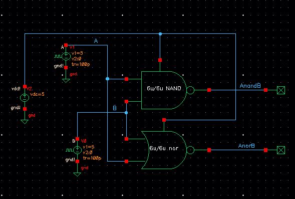
NAND gate schematic
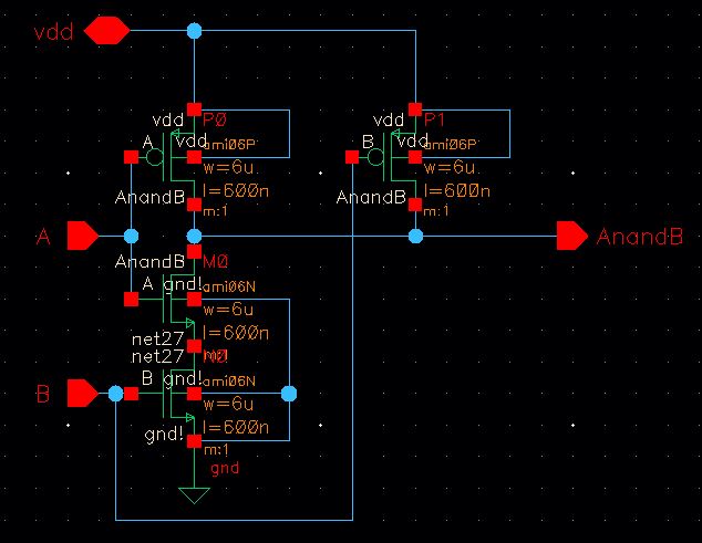
6u/6u NOR schematic
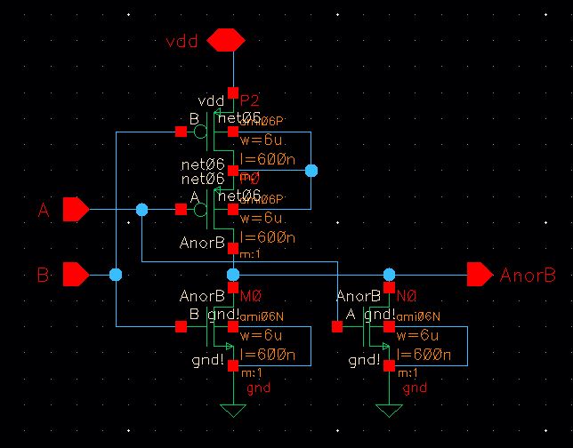
6u/6u NAND/NOR simulation schematic
6u/6u NAND/NOR simulation results
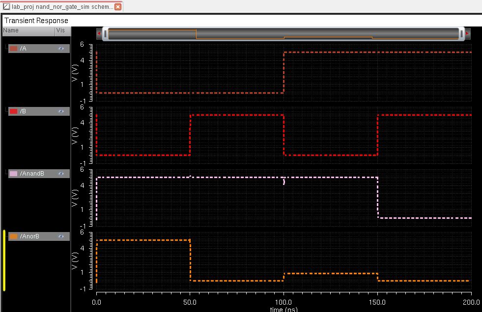
The
simulation of the two gates consisted of feeding all 4 possible
logic combinations of the inputs to each gate (00,01,10,11). The results are
as expected, the only time that the NAND output is low is when both
input signals are high and the only time that the NOR gate output
is high is when both inputs are low.
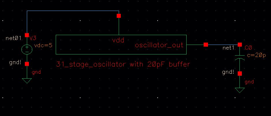
31 Stage Oscillator
Below
is the schematic & simulation of a 31 stage ring oscillator with an
output buffer driving a 20pF load. The inverters outside the inverter
array (using an A multiplier of 8 & a stage of m=64) are used as an output buffer so that the oscillator can drive a
20pF load.
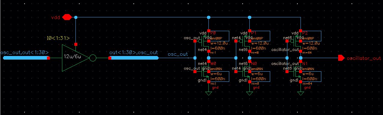
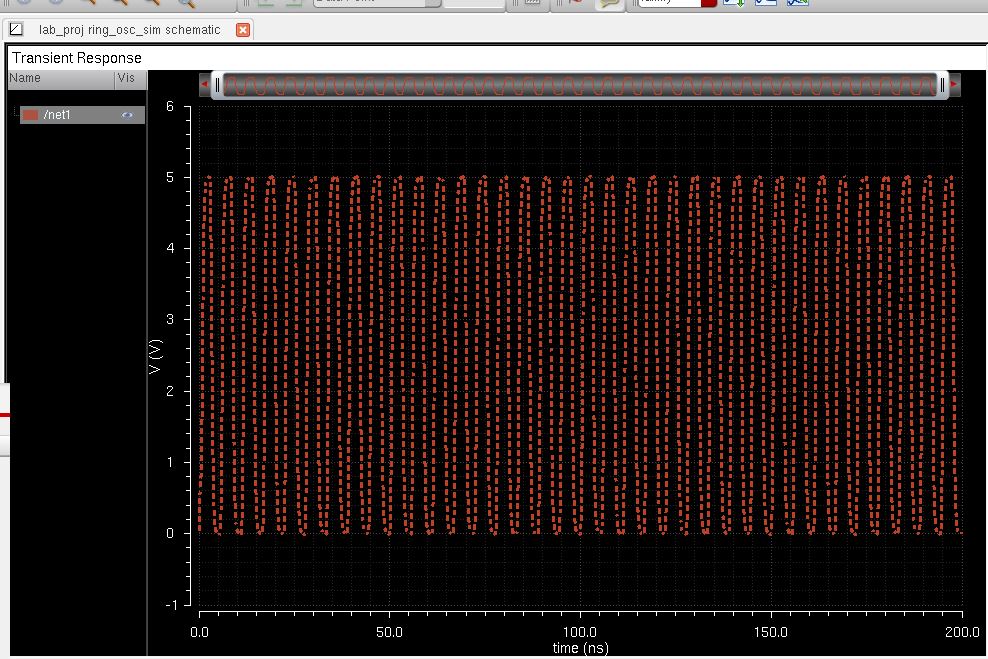
Oscillator simulation schematic
From the simulation one can see that period of the oscillator
is roughly 5ns, which translates to a frequency of 200Mhz (T=1/f).
8-bit Resettable Up/Down Counter:
The
basic building block of a Resettable Up/Down counter is a D flip flop
with a clear. Below are the pictures showing a D flip flop with a clear
and the simulations.
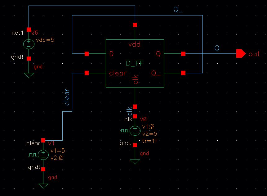
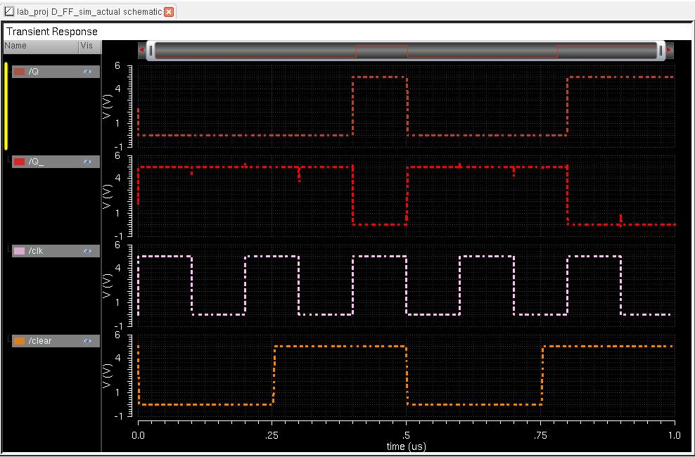
Schematic of a resettable D-FF
D-FF simulation schematic
Simulation results (showing clear when high & low)
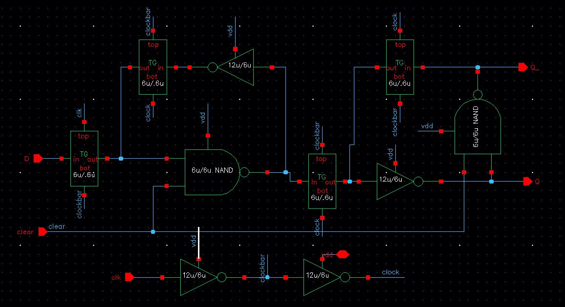
Below are pictures showing the schematic of an up/down counter utilizing the D-FF & transmission gates.
1-bit up/down counter
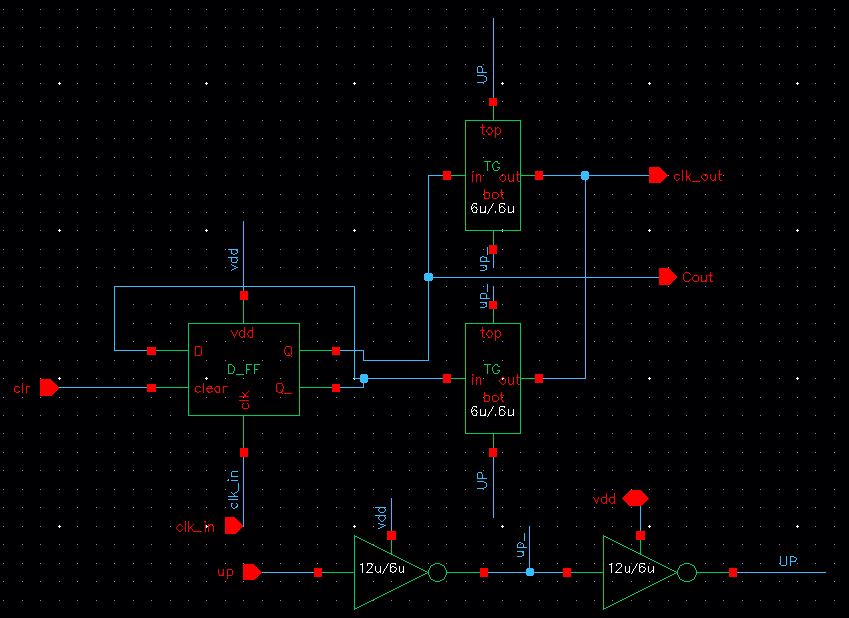
8-bit up/down counter
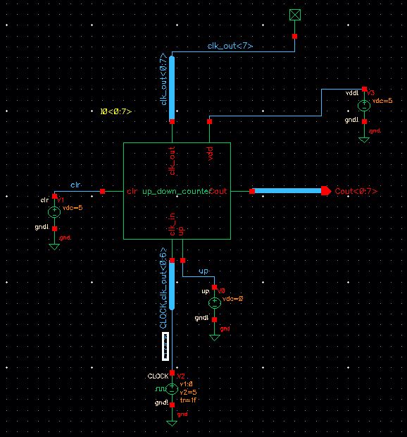
To
go from a single bit up/down counter to the 8 bit counter, simply
create a symbol for the 1 single bit. Then use the 1-bit counter symbol
& modify it's properties to have an array from <0:7>. Then by
using buses, connect wires to the right locations by using proper
labeling of the buses. Then you can simply create a symbol of the 8-bit
counter for testing.
The
functionality of the up/down
counter is that when an input with signal high (VDD) is fed into
the
up input, the counter will count up. When a input signal low (GND) is
fed into the up input, the counter will count down. Also whenever a low
is fed into the CLR, the counter will clear all it's registers to
0 and start up or down counting from 0 once the CLR signal goes back to
high.
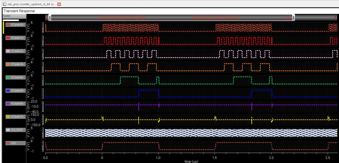
8-bit counter counting down from 255 to 0.
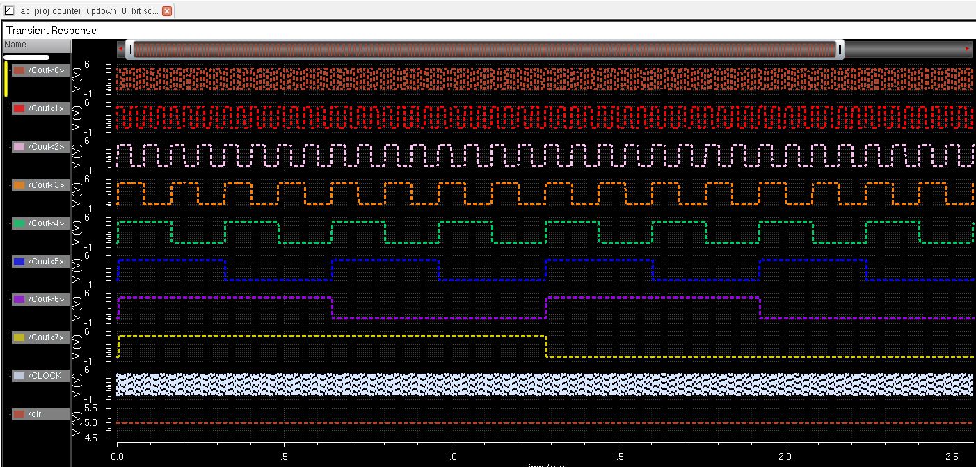
8-bit counter counting up to 255.
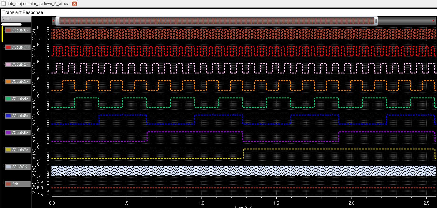
Counting up with clear
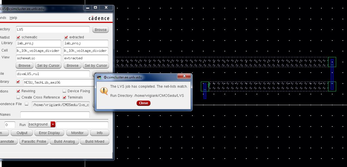
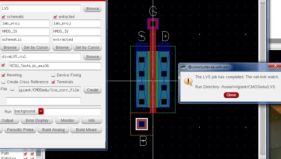
Below are the layouts to the cells shown above.
Voltage divider
NMOS
PMOS
Inverter 12u/6u
NAND
NOR
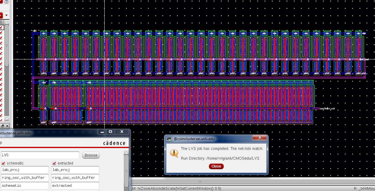
Ring oscillator with 20pF buffer
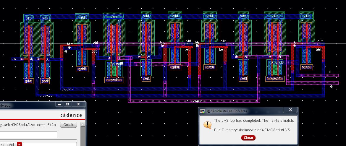
D Flip Flop
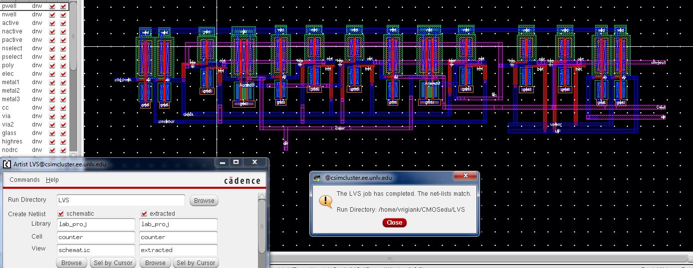
1 bit counter
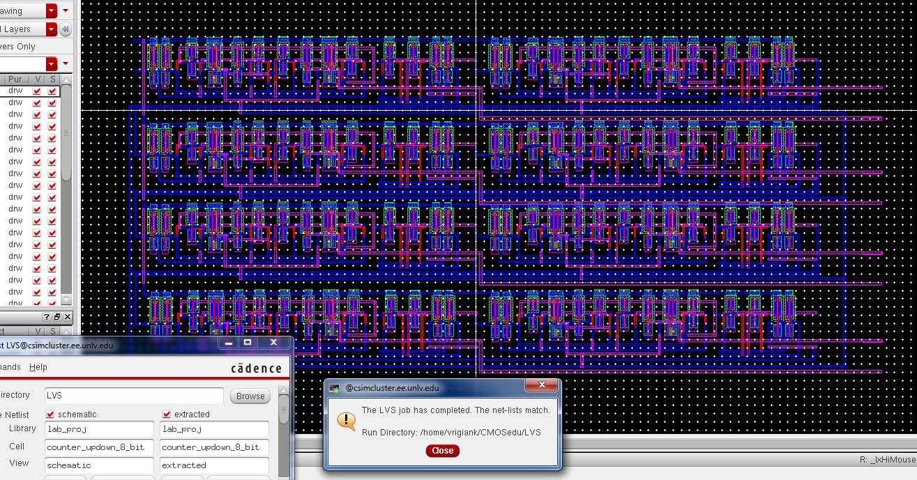
8-bit counter including up/down
All of the files for this lab can be found here.
Be sure to backup all your lab by uploading it to a drive or online.
Return to EE 421L Labs