Lab 4 - EE 421L
Vrigiank@unlv.nevada.edu
Kirk Vrigian,
9/25/15
In
this lab we will layout a NMOS & a PMOS, also we will learn
how the gate, source, & drain of a NMOS & PMOS are related to
their respective drain current.
First,
copy your Tutorial_1 folder into a new library called tutorial_2 (right
click tutorial_1 and click copy, name new location tutorial_2).
Now create a new cell view in Tutorial_2 called NMOS_IV, a 4 terminal transistor.
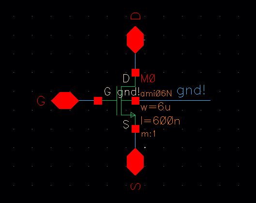
Create
an instance from the NCSU_Analog_Parts library & in the
N_transistors then selecting nmos4. Set the transistor's width to 6u
& the length to 600nm, then place in your schematic.

Next add pins with the direction of InputOutput as well as wires like the image below.
Then,
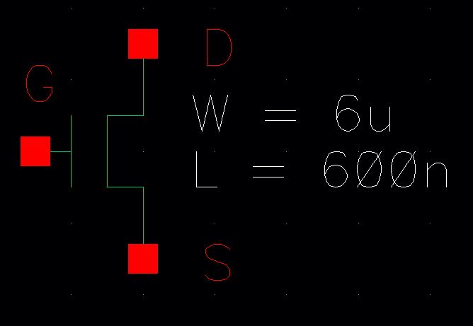
create a symbol view for the schematic by going to Create -> Cell
View -> from Cell View. Select all the pins & open the property
window (q). Use the drop down menu for "Apply To' and click 'all
selected' & change the display to 'value'.
Draw
the MOSFET symbol similar to the image below. Add text for quick
reference by using Create -> Note -> Text, then save.
Close
any open schematics or symbols & return to the Library Manager to
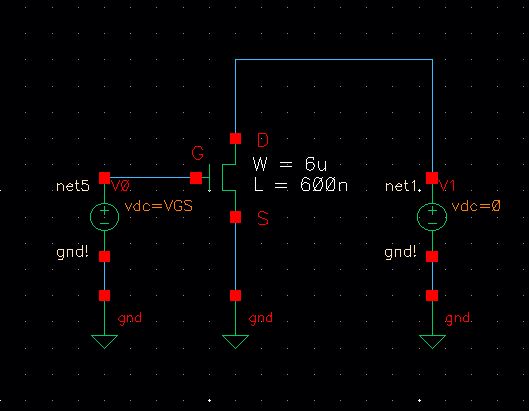
create a new cell view called sim_NMOS_IV. Instantiate the NMOS_IV
symbol & create a schematic like the one below. Set the V0 vdc =
VGS and the V1 vdc = 0. Save obviously
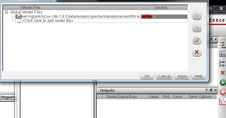
Now
launch ADE. Go to Setup -> Mosel Library & add ( clicking the
browse button that has '...' on it) the ami06N.m from the
/$HOME/ncsu-cdk1.6.0.beta/models/spectre/standalone. For a PMOS use the
ami06P.m.
Go
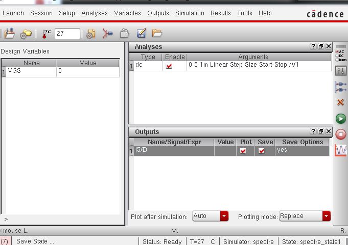
to Variables -> Edit & add VGS as the name & 0 for the
value. It will show up in the design variables window in ADE.
Now setup a dc sweep like below.
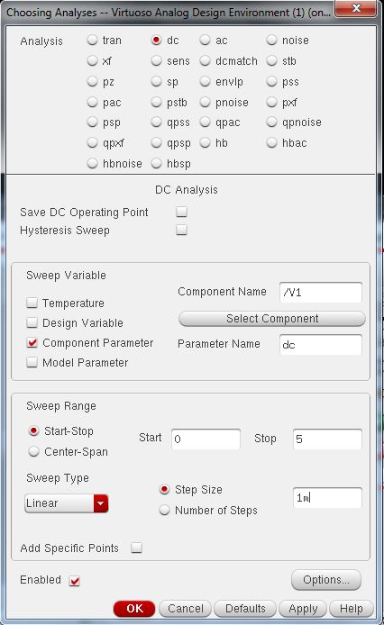
Select the D-pin on outputs to be plotted & verify that both plotted & save are selected.
Save
the simulation and then go back to the ADE window & choose Tools
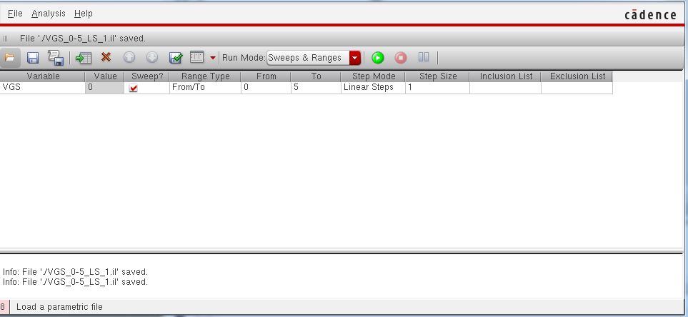
-> Parametric Analysis & set the parameters as seen below.
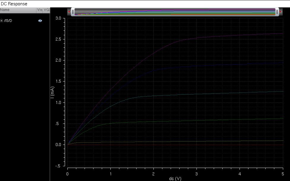
Now click the green play button to see the IV curves of the MOSFET (seen below).
Now we save the state and close the schematic.
Now we create the layout for this cell & simulate it.
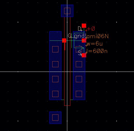
First create a new cell layout labeled NMOS_IV
Next,
instantiate the nmos4 layout and set it to 6um wide & 600nm long.
Add a ptap cell, and add rectangles of metal1 to connect the source to
the p-substrate & to the drain. Also instantiate a m1_poly &
and draw a poly rectangle to connect the gate to the m1_poly. Add D, G,
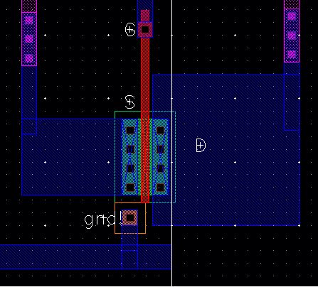
& S InputOutput pins on metal1. DRC & save the cell view,
extract the layout & open the extracted cell view to see the symbol
which has 4 terminals, this symbols helps show where all the pins are
and where they are going.
NMOS_IV
layout with no DRC errors.
Extracted view

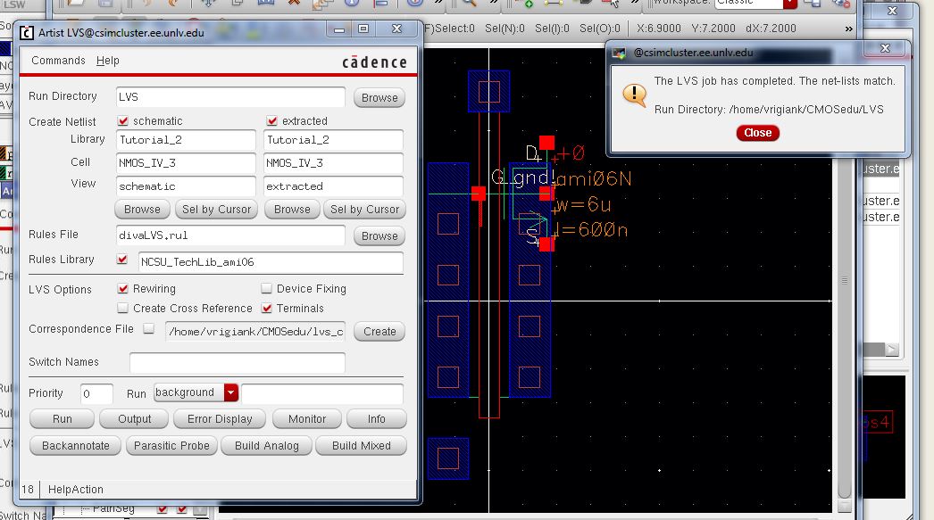
Now LVS the extracted NMOS_IV with the schematic of the NMOS_IV, the netlists should match.
Now let's simulate the extracted layout instead of the schematic of the NMOS_IV.
Open the schematic view of the sim_NMOS_IV & launch ADE L.
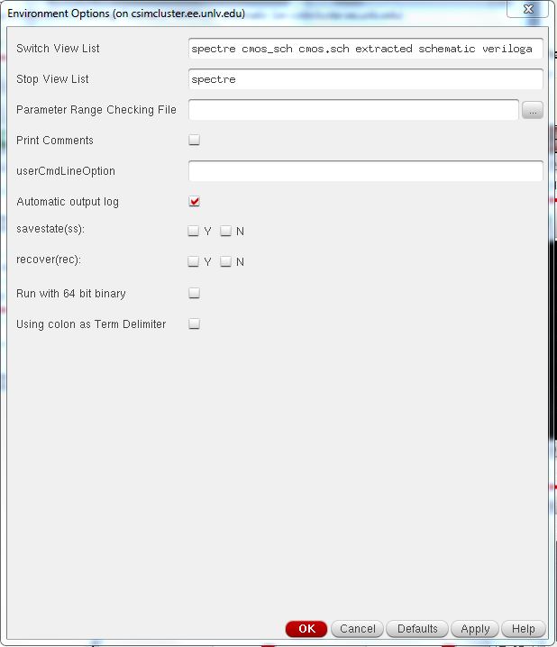
Load
the state from cell view and go to Setup -> Environment & type
extracted before schematic in the Switch View List. This is so the
program will defer to the extracted view for simulation before the
schematic. Warning: if you don't delete this extracted from the box,
all your sims will continue to run extracted simulations if they have
them.
Run the same parametric analysis & the exact same results will occur, assuming the layout/extracted file is done correctly.
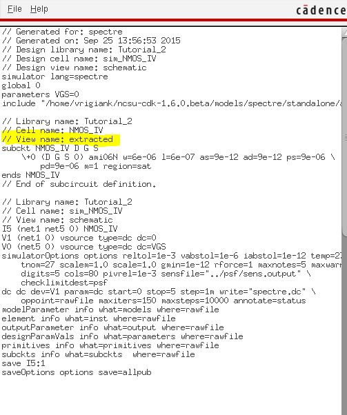
To
verify that cadence actually simulated using the extracted view &
not the schematic view go back to the ADE window & go to Simulation
-> Netlist -> Display & you will see the View name is
extracted.
Now we must do the same process for a PMOS device.
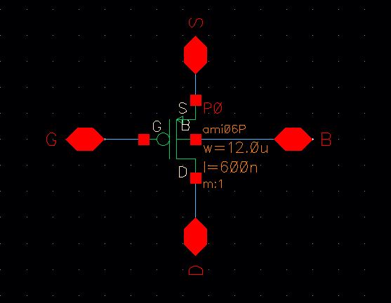
Create a schematic cell view called PMOS_IV
Instantiate a 4pin pmos & make the width 12um & the length 600nm.
Add the proper InputOutput pins as seen below.
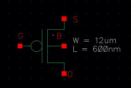
Create a symbol for the schematic, be sure to check & save.
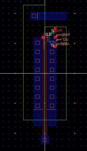
Create a new layout for the PMOS_IV as well. DRC and extract (same as before with the NMOS).
PMOS_IV
layout
Extracted PMOS_IV

Save & close the extracted view and layout view.
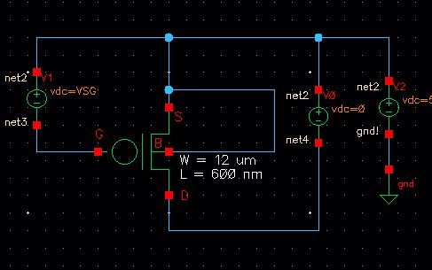
Create a new cell called sim_PMOS_IV & draft the following schematic
PMOS_IV simulation schematic
Check
& save. Then launch ADE & go to model libraries again and
select the PMOS models for AMI06 this time. Go to variables -> Edit
& add VSG with a value of 0.
Then select the outputs & the source terminal of the transistor having both Plot & Save selected.
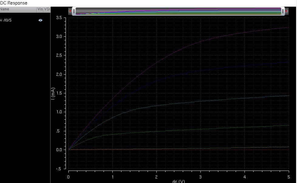
Run the parametric analysis (same settings as before but changing your variable to VSG).
PMOS_IV IV curve with schematic
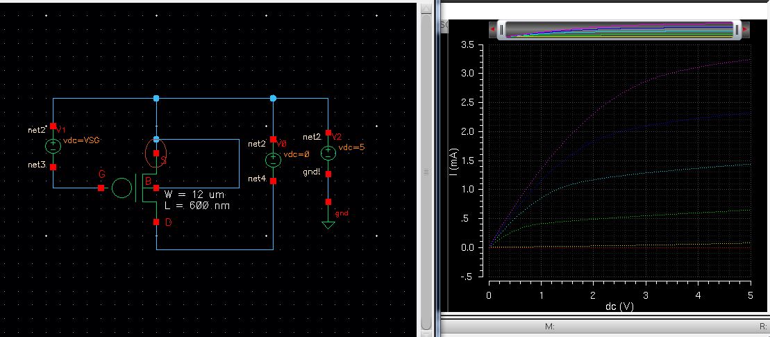
Do the same simulation but using the extracted layout, you should get the exact same results.
PMOS_IV IV curves
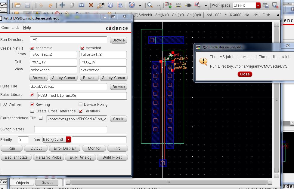
LVS the extracted view with the schematic view.
LVS of the extracted PMOS_IV
Now we have sucessfully created a symbol and a layout of a NMOS and a PMOS
We can now take a look at some NMOS relations.
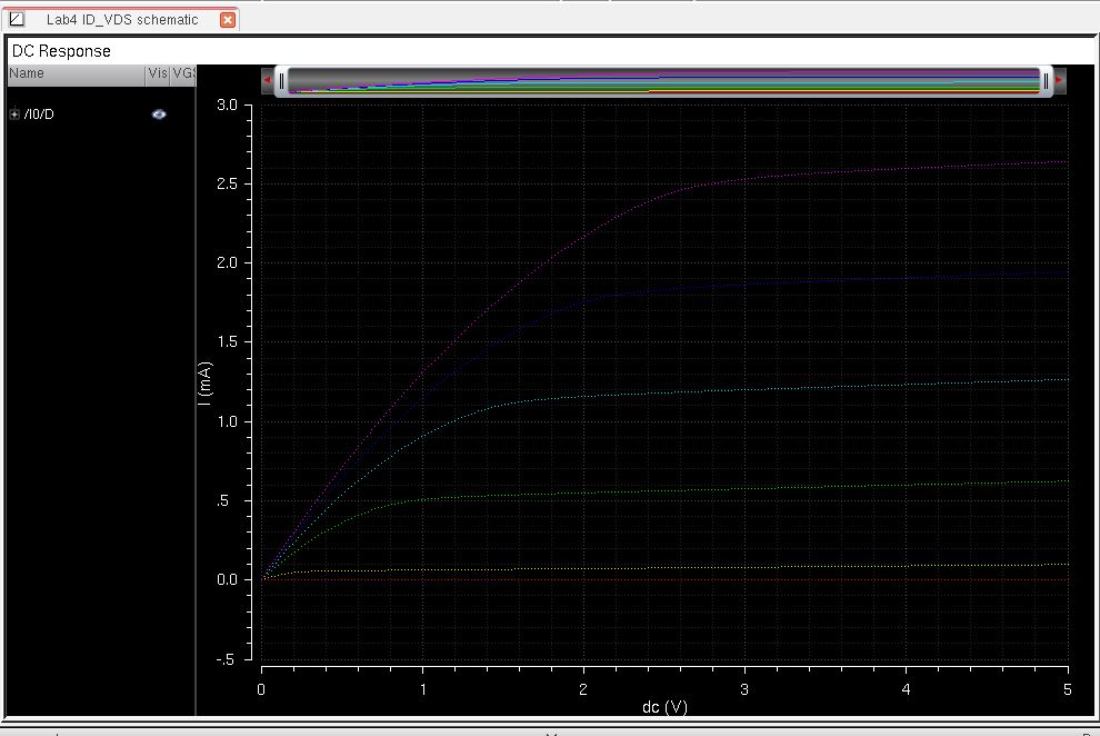
First let's take a look at the
curve of ID versus VDS of an 6u/600n w/l NMOS device when the VGS
varries from 0 to 5 V in 1 V steps, and when VDS varies from 0 to 5 V
in 1mV steps.
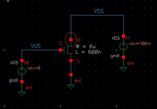
Create a schematic cell view in your lab4 library, name it ID_VDS.
Draw the following schematic seen below, we are using the NMOS we created previously.
Check & save your schematic.
Open
ADE L. Choose ami06 as your model library for the NMOS. Then create a
dc response according to the type of response we noted above. Create a
design variable named VGS & set the value to 0. Select your output
variable as the drain pin.
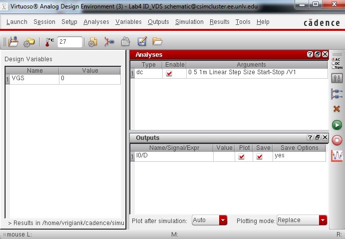 Run the same parametric analysis for VGS with value of 0 from 0-5V with step size 1.
Simulating it will result the following graph.
 Secondly let's take a look at the curve of ID versus VGS of an 6u/600n w/l NMOS
device when the VGS varries from 0 to 2 V in 1 mV steps, and when VDS is 100 mV.
Secondly let's take a look at the curve of ID versus VGS of an 6u/600n w/l NMOS
device when the VGS varries from 0 to 2 V in 1 mV steps, and when VDS is 100 mV.Create a schematic cell view in your lab4 library, name it ID_VGS.
Draw the following schematic seen below, we are using the NMOS we created previously.
Check and save your schematic.
Now open ADE L.
Make sure you choose your model library in the ami06 as the NMOS.
Create a dc response according to the type of response we noted above.
Create a design variable name VDS and set the value to 0.
Make sure you select your Output variable as your Drain pin.
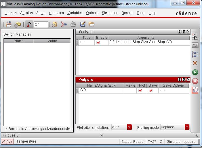
Running the dc response will result in the following graph.
PMOS relations:
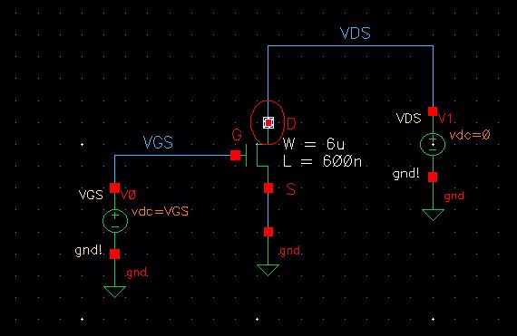
First
let's take a look at the curve of ID versus VSD of an 12u/600n w/l PMOS
device when the VSG varries from 0 to 5 V in 1 V steps, and when
VSD varies from 0 to 5 V in 1mV steps.
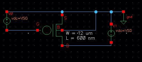
Create a schematic cell view in your lab4 library, name it ID_VSD.
Draw the following schematic seen below, we are using the PMOS we created previously.
Check and save your schematic.
Now open ADE L.
Make sure you choose your model library in the ami06 as the PMOS.
Create a dc response according to the type of response we noted above.
Create a design variable name VSD and VSG and set both of their values to 0.
Make sure you select your Output variable as your Source pin.
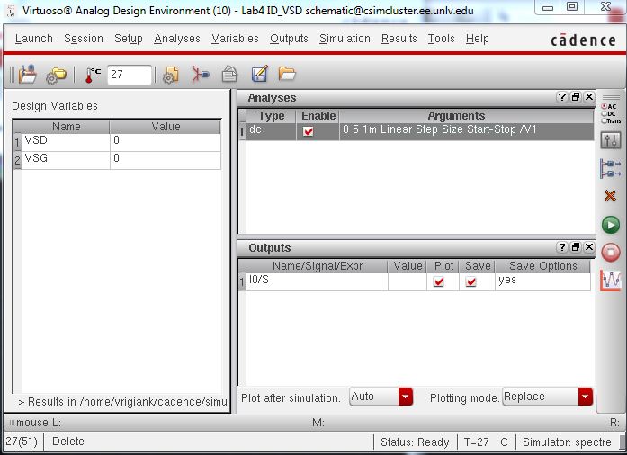
Go to Tools and Parametric Analysis again.
Set up your values seen below and run the analysis.
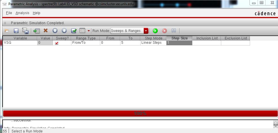
The analysis will result in the following.
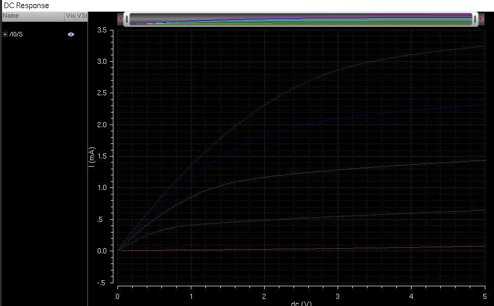
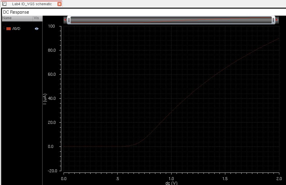
Lastly, let's take a look at the curve of ID versus VSG of an 12u/600n w/l PMOS
device when the VSG varries from 0 to 2 V in 1 mV steps, and when VSD is 100 mV.
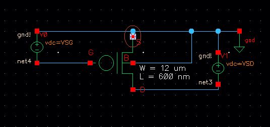
Create a schematic cell view in your lab4 library, name it ID_VSG.
Draw the following schematic seen below, we are using the PMOS we created previously.
Check and save your schematic.
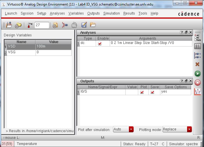
Now open ADE L.
Make sure you choose your model library in the ami06 as the PMOS.
Create a dc response according to the type of response we noted above.
Create a design variable name VSD and VSG and set their values to 100m and 0 respectively.
Make sure you select your Output variable as your Source pin.
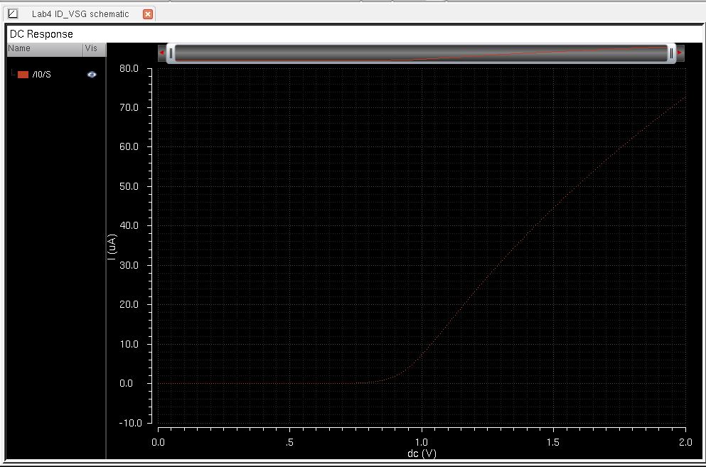
 Running the dc response will result in the following
Now let's layout a NMOS and PMOS.
First we have to create a probe pad.
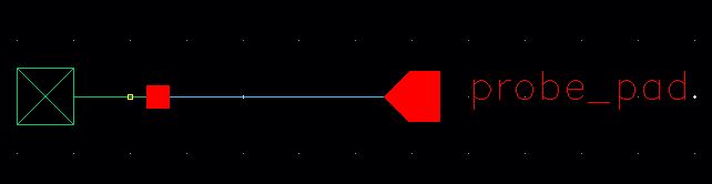
Create a new schematic cell view in your lab 4 named probe_pad.
Draw the following schematic.
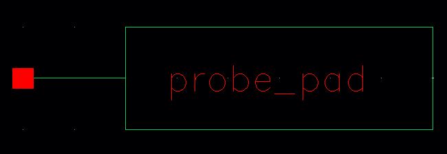
Create
a symbol from the cellview and delete everything except what you see
below. This is now our symbol for a probe pad we can use in the
schematic of our NMOS and PMOS.
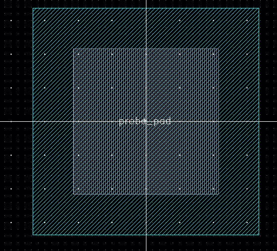
Create a new layout view in your probe_pad cell and layout.
Lay out a sheet of n-well that is made out of metal3 that has a width and height of 33.6um.
And lay out an over glass that 21.6um square.
Now let's start with a NMOS layout.
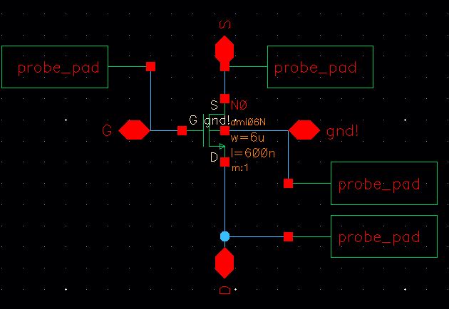
We are going to layout a 6u/0.6u NMOS and connect all of 4 MOSFET terminals to probe pads.
Create a new schematic view called 6u_600n_NMOS.
Draw the following schematic using the NMOS from Tutorial_2 and the probe_pads symbol you just created.
Check and save your schematic.
Create a new layout view and lay out the following layout.
We are using the layout probe pads we created before and the NMOS we created in Tutorial_2.
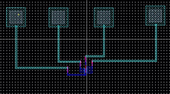
Connect the Source, Drain, Gate and gnd! with metal 1 pins to corresponding pads.
Save and extract your layout.
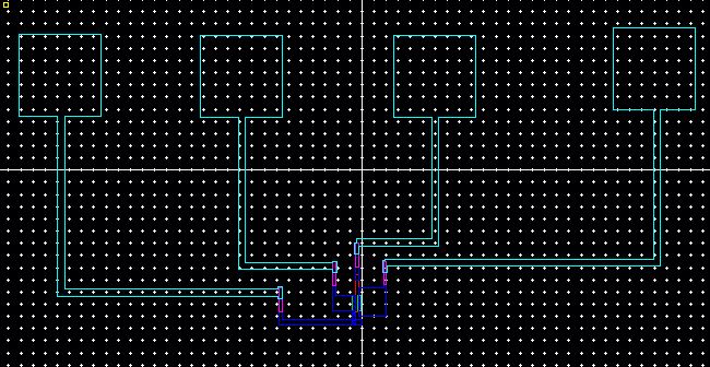
Open your extracted layout and it should look like the following.
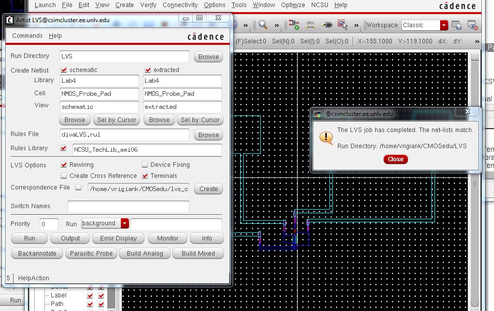
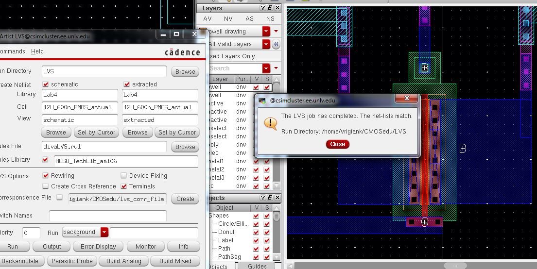
Now LVS your extracted view with the schematic view you created earlier.
Make sure you select the correct extracted and schematic file.
Run the LVS. The netlists should match.
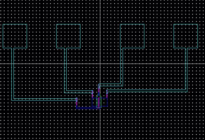
Now let's make a PMOS layout.
We are going to layout a 12u/0.6u PMOS and connect all of 4 MOSFET terminals to probe pads.
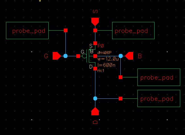
Create a new schematic view called 12u_600n_PMOS.
Draw the following schematic using the PMOS from Tutorial_2 and the probe_pads symbol you just created.
Note that the pin labeled B is your vdd! pin.
Check and save your schematic.
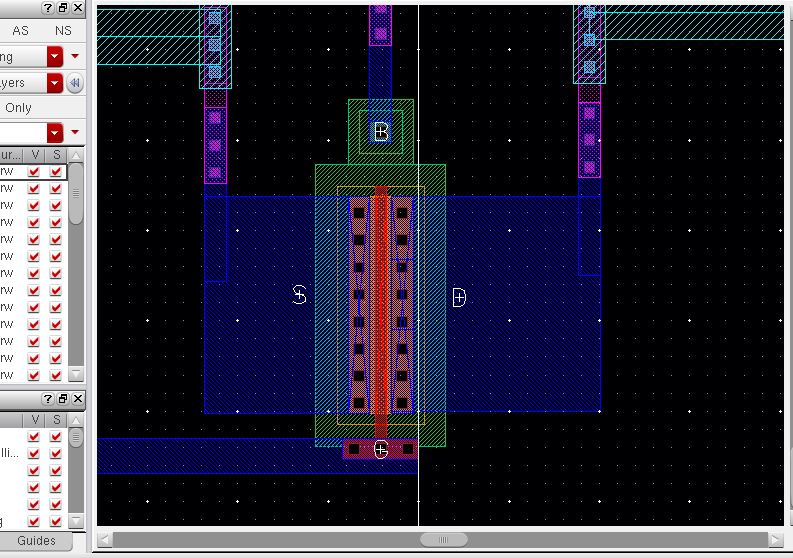
Create a new layout view and lay out the following layout.
We are using the layout probe pads we created before and the PMOS we created in Tutorial_2.
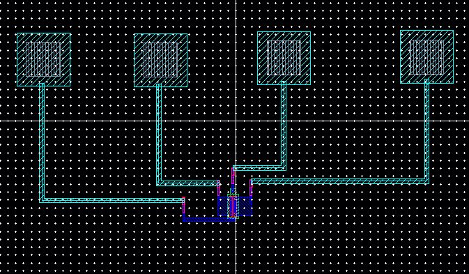
Connect your Source, Drain, Gate, and B with metal1 pins.
DRC & Verify it works
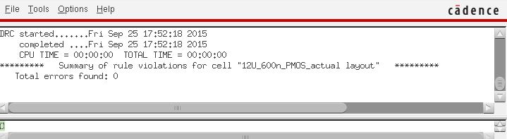
Now we can extract our layout. Then LVS the extracted view with the schematic, netlists should match.
All of the files from this lab can be found here.
Finally, back up your lab work by zipping it up & uploading it to a drive.
 Return to EE 421L Labs