Lab 3 - EE 421L 

Vrigiank@unlv.nevada.edu

Kirk Vrigian,

8/18/15

  
Prelab:

    Back up all work 

    Read through & finish tutorial 1
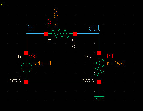


Lab 3 experiments & process:

In this lab we will learn to use layout in Virtuoso and create the 10 bit DAC we used in lab 2 with the layout.

First, copy everything from lab2 into a new lab3 directory. 

Now lets continue from where we left off in lab 1.


Open the schematic of the resistor divider, delete the bottom wire and the voltage source. Then, add another 10k ohm resistor after out followed by adding an "in" input pin an "out" output pin, and finally a "bot" input/output pin.

Original schematic

http://cmosedu.com/jbaker/courses/ee421L/f15/students/vrigiank/lab3/images/original%20schematic.jpg

Modified schematic

http://cmosedu.com/jbaker/courses/ee421L/f15/students/vrigiank/lab3/images/schematic.jpg

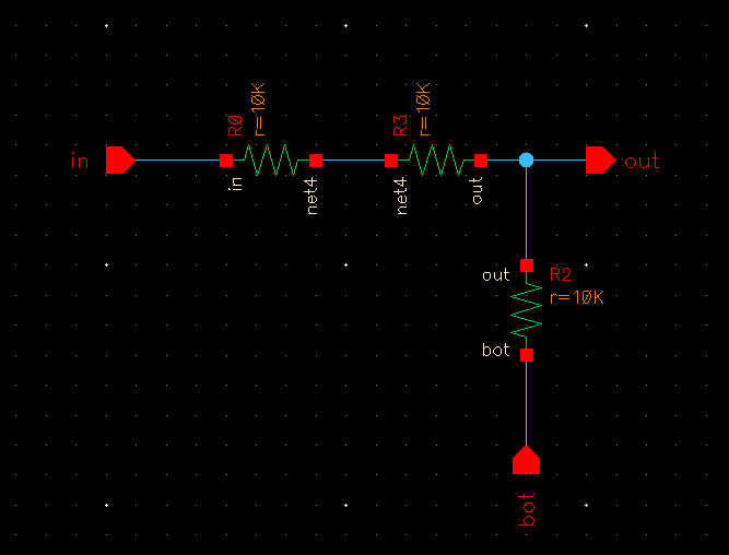
After checking and saving, the circuit is going to be made into a symbol for the convenience of having it as an instance. Go to Create -> Cellview -> From Cellview, draw your symbol and check & save.
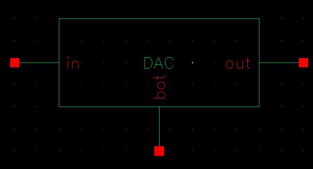
DAC symbol

http://cmosedu.com/jbaker/courses/ee421L/f15/students/vrigiank/lab3/images/dac%20symbol.JPG 

Then go to lab3, open the copy of the r_div schematic that you finished (with the pins), and delete everything in the cell. Import the symbol and attach a 1v source and wires to in & out then check & save. You will get floating errors, just ignore them so you can check & save. 

Launch ADE and load the state from cellview and run the transient response. You should get the same graph from your resistor divider your made in lab 1.
Save and close out of the copy_R_div. 

Now create a new cellview for the layout of our divider. Ensure that all layers are visible (AV) in your layer selection window (LSW) and all select is on (AS).

Next go to Options -> Display (binkey e)

Select pin names in display controls & change display levels from start = 0 to stop = 10 

http://cmosedu.com/jbaker/courses/ee421L/f15/students/vrigiank/lab3/images/display%20settings.JPG

Now we create the shape in our layout. We are going to create a 10k resistor using n-well in layout. The sheet resistance of the n-well in the c5 process is roughly 800ohms. As for the design rules, the min width is 12 lambda (3.6u with lambda being 300nm or .3u). Our resistor width will be 4.5um & our length will be 56 um.

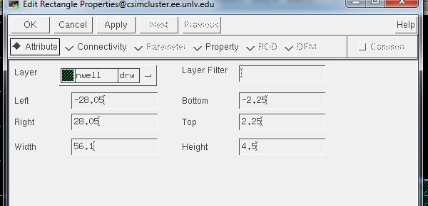
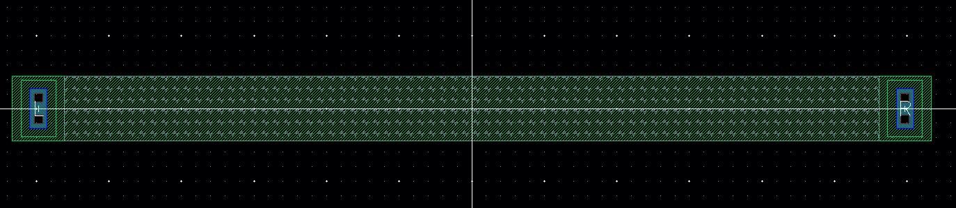
Create a new lout cellview call it R_n_well_10k. Select your nwell material in the LSW & press R to create a rectangle, draw any shape, then click the rectangle & press Q. This will open the rectangle properties where we want to set width to 56 & height to 4.5. Then DRC & save, it will have 4 errors, this is because the edge is not on grid. The rectangle needs to fit on a scale of .15u you can verify with the rule (bindkey k & bindkey shiftkey + k to remove).


http://cmosedu.com/jbaker/courses/ee421L/f15/students/vrigiank/lab3/images/ruler.JPG

Since the length is currently 56/0.15 = 373.333 this is not a whole number which means this is not a factor of 0.15 microns. We can increase the length to 56.1 since 56.1/0.15 = 374. Change the Left and Right values to 28.05. For the width it is 4.5 but since 4.5/0.15 = 30 it does correctly fit the 0.15 micron requirement.

Run DRC and you will receive no errors.


Final width & length scales

http://cmosedu.com/jbaker/courses/ee421L/f15/students/vrigiank/lab3/images/dimensions%2010k.JPG

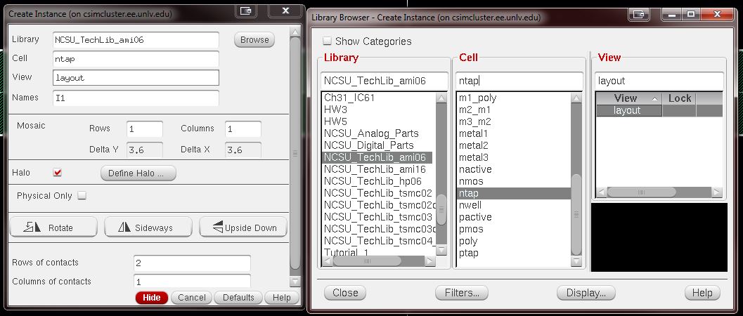
Now to add connections to the end of our n-well resistor. Press i to create an instance and navigate to ntap which is in the NSCU_TechLib_ami06 library.

Make sure you are changing the rows of contact to 2.

http://cmosedu.com/jbaker/courses/ee421L/f15/students/vrigiank/lab3/images/ntap.JPG

DRC your layout & verify there are no errors. Next add pins to the layout, select metal 1 on your LSW. Go to create -> pin & select display pin name, name your left pin L & and right pin R. Draw your pins on to of the metal1 rectangle on your ntap.
Next select the layer res_id in your lsw, draw a rectangle on top of your n-well rectangle, not including the ntaps. When you're finished you're resistor should look similar to this.

http://cmosedu.com/jbaker/courses/ee421L/f15/students/vrigiank/lab3/images/layout10k.JPG

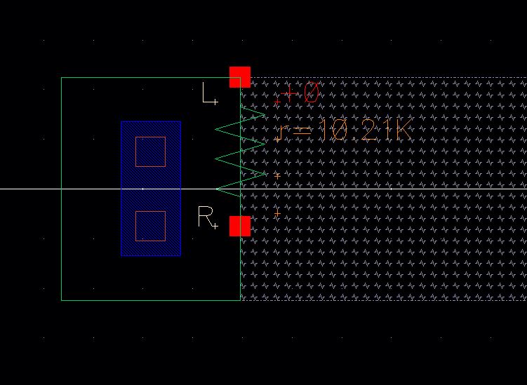
Now go to verify -> extract & click OK to find our resistance value.

Go to your library manager & open the extracted view in your R_n_well_10k cell. Zoom in and you will see your resistor's value is 10.21k

http://cmosedu.com/jbaker/courses/ee421L/f15/students/vrigiank/lab3/images/10_21k.JPG

Close the extracted view and the layout view of your resistor.

Create a new layout named mydesign_10-bit_DAC_layout

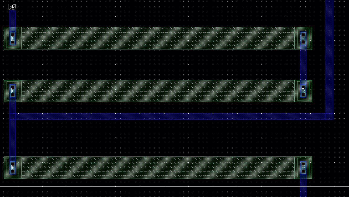
Istantiate two more 10k n-well resistor layouts. DRC your layout & ensure you have enough spacing between your resistors. Draw metal 1 rectangles from each resistor in series & one in parallel between the L of the 2nd resistor & the L of the 3rd resistor to simulate the out of the 1-bit DAC. These three resistors are essentially our 1-bit DAC or 2R-2R divider. Label & draw over the metal 1 rectangle on the top L pin as b0.

1 bit of the layout

http://cmosedu.com/jbaker/courses/ee421L/f15/students/vrigiank/lab3/images/1-bit%20layout.JPG


This will be our base design, we drc, extract & LVS this layout to make sure that it matches the schematic. After that, you will copy it and place 9 more bits & connect the parallel out (or top) to the bot of the next one. Label each input b1-b9 appropriately as well as the final parallel output as out.

Labeling the output pin of the top of the last DAC
http://cmosedu.com/jbaker/courses/ee421L/f15/students/vrigiank/lab3/images/out_b9.JPGhttp://cmosedu.com/jbaker/courses/ee421L/f15/students/vrigiank/lab3/images/out_b9.JPG

Do not forget to add one extra resistor below the 1st set of 3 resistors. This is also 10k, this alllows the first bit to be a 2R-2R design. Create a pin over the bottom L metal1 layer & label it gnd! and set it to inputoutput pin.

10k resistor attached to the bottom of the 1st DAC.
http://cmosedu.com/jbaker/courses/ee421L/f15/students/vrigiank/lab3/images/gnd_b0.JPG

If every pin is labeled properly, set to the right type of pin, and spaced appropriately enough, you will be able to DRC, extract, & LVS with no errors.

LVS of layout                                                                                                                              Extracted view of the 10-bit dac layout
http://cmosedu.com/jbaker/courses/ee421L/f15/students/vrigiank/lab3/images/LVS.JPG              http://cmosedu.com/jbaker/courses/ee421L/f15/students/vrigiank/lab3/images/extracte.JPG

The width and length of the resistor can be determined by using the equation of a resistor using R = L/W x Rsq where Rsq is the sheet resistance of the material, in this case it is 800 ohms in the C5 process.

If we rearrange the equation looking for L/W = R/Rsq
Where R = 10k ohms and Rsq = 800 ohms

We get the ratio of L/W to be 12.5

Letting us really pick any value of length and width be whatever aslong as the ratio is around 12.5

For our 10k n-well resistor we used 56.1 microns for the length and 4.5 microns for the width which is 56.1/4.5 = 12.4666

Since we used the 10k n-well resistor we created for the 10-bit DAC we already know the measurements of each 10k resistor.

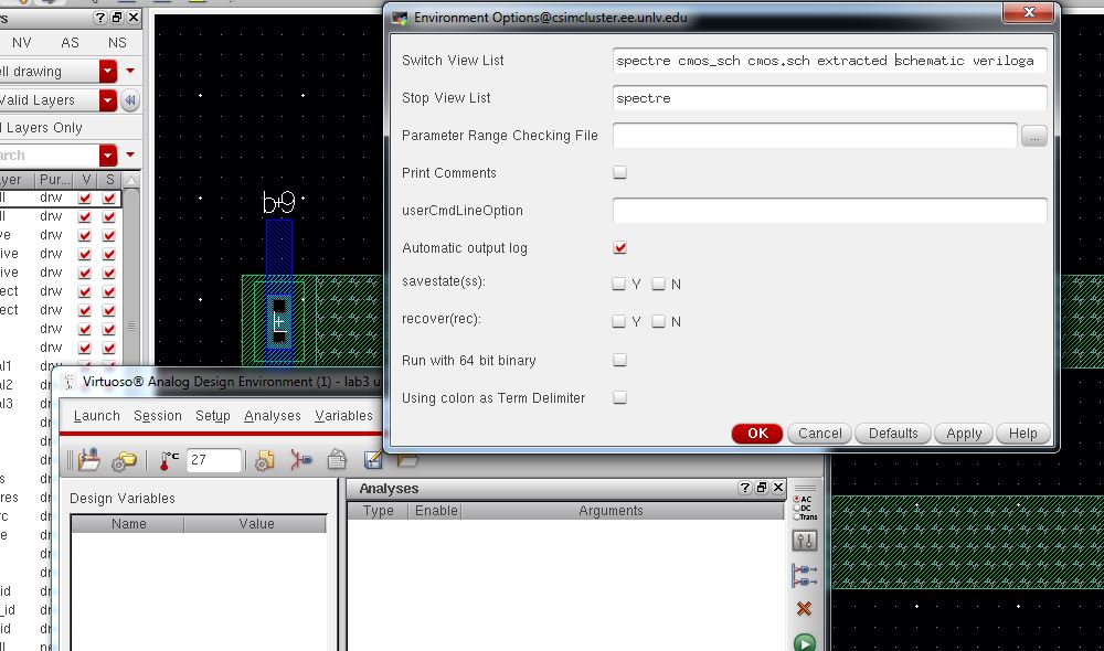
If we edit our simulation options to run the extracted before our simulation we can test & compare our results to our lab 2 DAC. Our results should be and are very similar. You can do this by clicking ADE L -> Setup -> Environment and typing "extracted" before schematic in the box.

ADE L settings

http://cmosedu.com/jbaker/courses/ee421L/f15/students/vrigiank/lab3/images/settings.JPG

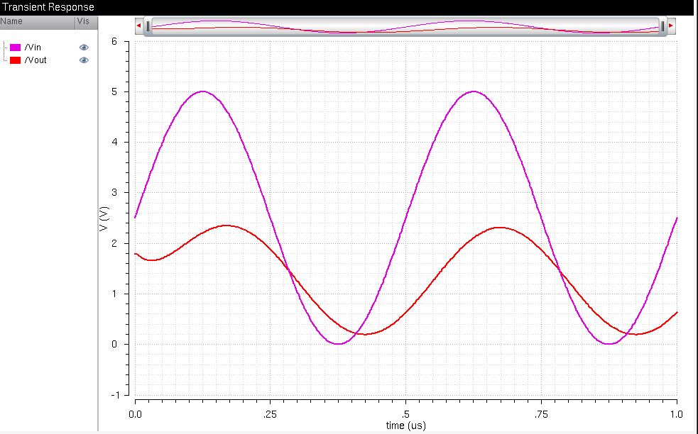
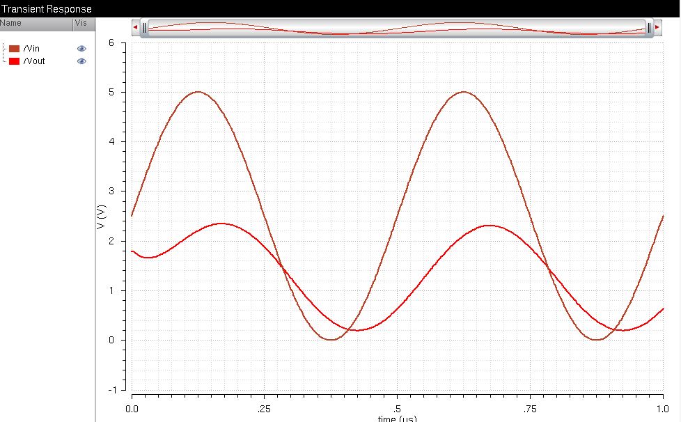
Simulation results of our extracted layout driving the same 10pF capacitor and 10kOhm resistor. Results are the same from lab2

Lab 3 extracted results

http://cmosedu.com/jbaker/courses/ee421L/f15/students/vrigiank/lab3/images/capacitor_resistor%20sim.JPG  

Lab 2 results
http://cmosedu.com/jbaker/courses/ee421L/f15/students/vrigiank/lab2/10k10pf%20sim.JPG


You can download the schematic of my 10-bit DAC, my 10k n-well resistor and my 10-bit DAC layout using the 10k n-well resistors here.

Be sure to backup your files & images, as usual.

http://cmosedu.com/jbaker/courses/ee421L/f15/students/vrigiank/lab3/images/upload.JPG

Return to EE 421L Labs