Lab 2 - EE 421L
Vrigiank@unlv.nevada.edu
Kirk Vrigian,
8/29/15
Prelab:
Back up all work
Read through entire lab write-up
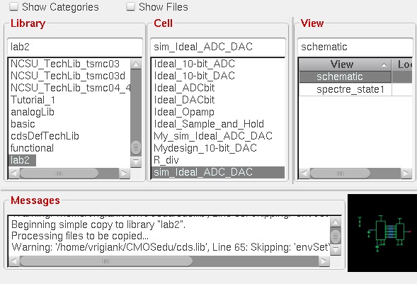
Download lab2.zip
Contains a simulation example of an ideal
10-bit Analog-to-Digital Converter (ADC) & Digital-to-Analog
Converter (DAC)
Upload lab2.zip to design directory and extract
Add 'DEFINE lab2 $HOME/CMOSedu/lab2' to cds.lib
Execute cadence from design directory
Image contains extracted lab2.zip, virtuoso & command, & 'DEFINE lab2 $HOME/CMOSedu/lab2' script to cds.lib

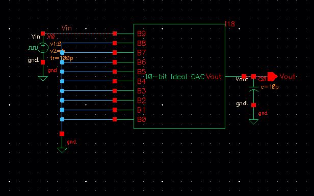
Open the schematic view of the cell sim_Ideal_ADC_DAC
This cell contains the ideal 10-bit converters.

Run a transient response simulation of Vin & Vout
The way an analog-to-digital converter works is by receiving an analog
signal, and converting the output to a digital signal which are bits. A
digital-to-analog converter functions the same way just inversely so.
One thing to note is that due to Vdd, the output of the circuit is
limitied, so regardless of what amplitude one uses for Vin, the circuit
will still clip and clamp at 5V.
This circuit is a 10-bit DAC/ADC circuit which means that the total number of possible bits is 210, all of which scale between 0V & 5V, the more bits, the more granularity in the output.
Calculating the step voltage would be Vref/2n or in this case, 5V/1024 = 4.88mV
Image shows the approximate step voltage between input and output

In order to calculate the LSB one uses the defintion or equation
LSB= Vref/2N where N = the number of bits, or in this case LSB = 5/1024 = 4.883mV
We can see this graphically by plotting the lowest
pin and the highest pin to see which one is the LSB.
Graphically the LSB changes much more frequently than the MSB which makes sense as the LSB only needs every 4.883mV to change.

As shown in the graph and circuits, Vin is an analog input in the form of a sinewave
The analog signal is entered into the ADC, which
discretizes it in the form of the 10 bit pins, based on the voltage
level
The digital signal is then fed into the DAC which
reforms the signal into a series of steps to best replicate the
original signal.
An increase in bits can increase
the granularity or accuracy of the signal, but it will never be exact

Lab 2 experiments & process:
Now
that we know how the ideal ADC & DAC out puts look, lets
modify the DAC. First, copy the Ideal_sim_ADC_DAC & Ideal_10-bit-DAC, these will be modified for our simulations.
Next, from the Library manager click on lab2 library, then click file->new->cell view.
Create a new cell view schematic called R_div. This will be your 1-bit
DAC. It should be similar to the layout below. Use 10K resistors only.
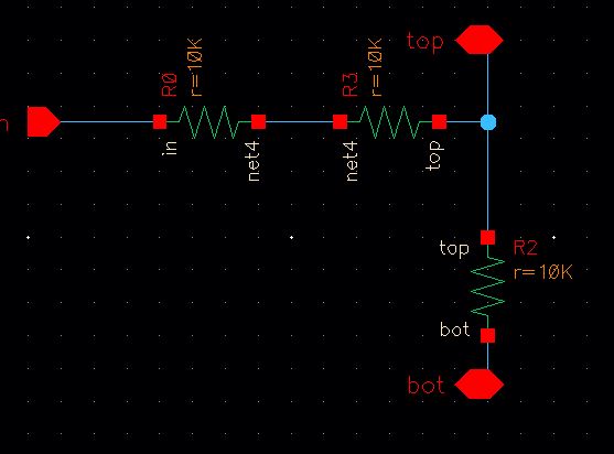
Once the schematic has been properly created, ensure you check & save, then create a symbol from the schematic. Go to create->cell view->from cell view. This will create a symbol to use in your 10-bit DAC, be sure to check & save.
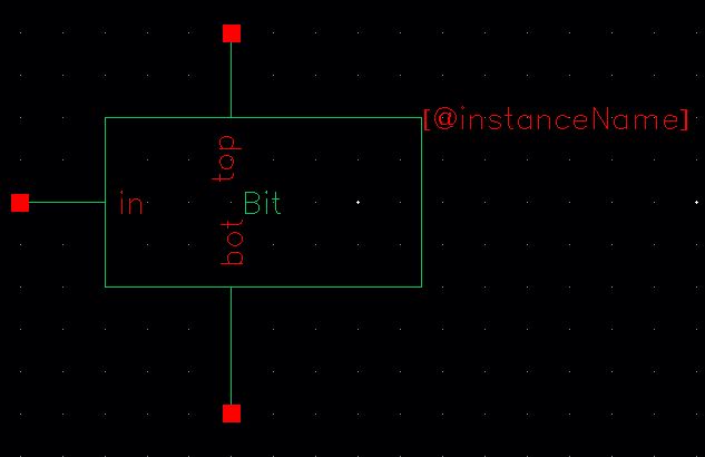
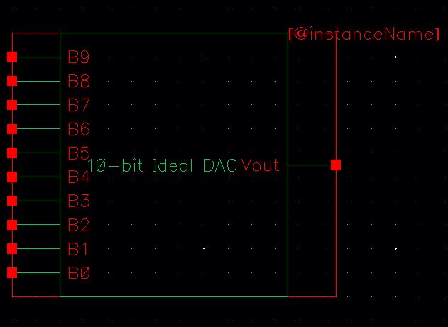
Now open the copy of the Ideal 10 bit DAC symbol and modify it. Replace all the 1bit
DAC with the ones just created. The updated schematic and
symbol should be similar to the images below.
10-bit
schematic
10-bit symbol

The
total resistance of the 2R and R circuit calculated to R. This cascades and repeats so the entire output resistance
can be easily calculated. Starting from the bottom of the circuit, the resistance of 2R and 2R in parallel
become R, (2R * 2R)/(2R
+ 2R) = R. This R is added to the resistor above. Which adds to 2R, which is now in parallel with the 2R to the left of it. Like stated earlier, this is cascaded, untill we are left with a lone pair of 2Rs, which is finally
just R.

Now
that the 10-bit schematic & symbol are created, we can replace the
old DAC symbol in our copy of the ADC DAC schematic. The new DAC
obviously has fewer pins, this is okay.

Simulate
the circuit using a transient simulation with time of 1us (same as the
original ADC_DAC simulation). The results are similar, the image below
shows that there is
still an analog to digital to analog conversion occuring.

Now, inplement a 5 volt pulse to the B9 input port, ground B0-B8, and finally connect the output to a 10pF capacitor.
By only utilizing the B9 port, we will get a binary value of 512, out of
our 2^10 values, or in other words 1024. This will half
of the voltage input, 5V * 512/1024 =2.5V. The td = 0.7RC, which is approximately at 50%, in our case this is, 0.7 * 10pF * 10,000Ohms, which will be 70nS.
Td simulation

ADC_DAC driving a 10k load

The
simulation shows the output from the DAC driving a load of 10k. The
output is around 2.5 v mark when the input is at 5v. This is happening
because the 10k resistive load is in series with the 10k resistance
total of the DAC circuit. This creates a voltage divider with a ratio
of 1/2,output to input.

Schematic of the circuit now driving 10pF

The
output has become smoother, but the amplitude is slightly reduced. The reduction in amplitude occurs
due to the impedence of the capacitor. The
smoothness of the output is due to the accumulation of voltage rising in the
capacitor.

The circuit driving a 10k resistor in parallel with a 10p farad
capacitor.

This
circuit combines the 'smoothing' of the capacitor, with the voltage
reduction of the resistor.

In a real circuit the switches in the ADC DAC circuit (the outputs of the ADC) are
implemented with transistors (MOSFETs). Discuss what
happens if the resistance of the switches isn't small compared to R.
If
the resistances of the switches are not small compared to R, then the
switches would hinder the DAC unit of the proper voltage necessary
to output a decently quantized value, reducing the output
to approximately 1 minus the ratio of the switch resistances to DAC
resistances
percent. For example, if the switches' resistances where .01 of R, the
output voltage would be 1 - (0.01R/R) = 0.99, or 99 percent of the
original input. This change is negligible, however, if the switches
were a much higher value, for example, 50% of R, then the output
voltage would be 1- (0.5R/R) = 0.5, or 50
percent of the orignal value. This is a drastic change from the
accuracy of what we'd expect.
BACK UP THE LAB
So much time & effort, it would be a shame if it all somehow went missing.

 Return to EE 421L Labs