Lab 7 - EE 421L
Vrigiank@unlv.nevada.edu
Kirk Vrigian
10/25/15
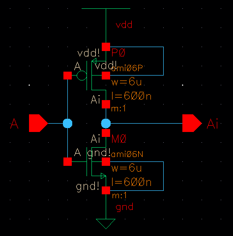
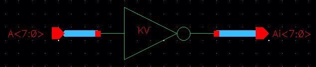
First create a 4x inverter using bus connections.
Do
this by instantiating the 12u/6u inverter used in lab5 & editing
the schematic to a 6u/6u ( the widths' for the PMOS & NMOS) Then putting our initials on the corresponding symbol.
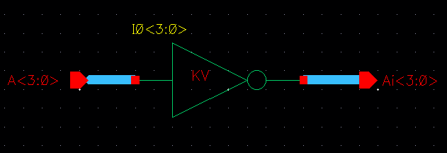
A
new schematic is created and the above symbol is instantiated. It has
its instance name changed to "IO<3:0>". This name change edits
the schematic into 4 inverters that are shown neatly and concisly using
the buse wire connecter.
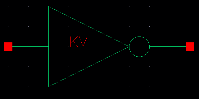
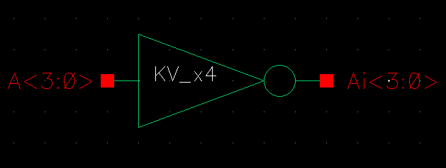
Now create a corresponding symbol for this schematic.
Now
create another schematic to simulate the x4 inverter with different
capacitive loads, the schematic should look similar to and have
the same results as below.
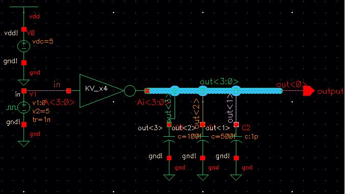
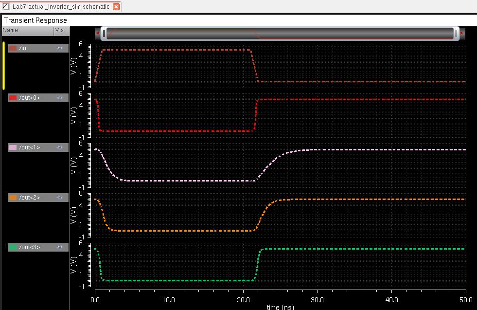
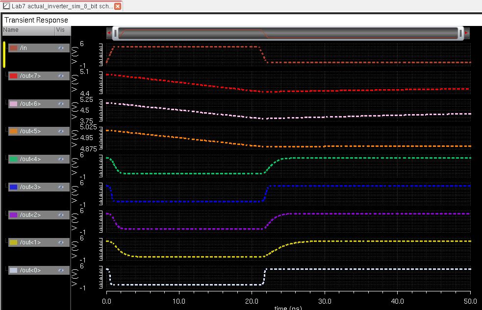
According to the simulation results, a larger capacitance,
results in a longer required time for discharging/charging. This is due
to the time constant RC. For example, the time delay in a RC
circuit is defined to be 0.7RC. Since the capacitance is bigger,
the 0.7RC equation increases, which increases the delay. This is best
shown on the above simulation results in the output "out<1>",
which has the biggest capacitave load. In this output, the wave form
has more of a "slope" on its rise time, which indicate that it
takes longer for it to charge/discharge. In contrast, "out<3>" ,
which has the smallest capacitive laod, has a smaller rise/fall
"slope", which indicates that it keep up with the change of the input
since it is does not reqire as much time for charging/discharging.
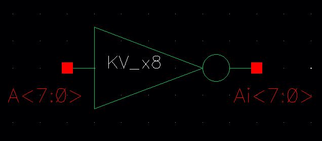
Next, repeat the process but create an 8-bit inverter schematic & symbol.
symbol
Simulation schematic
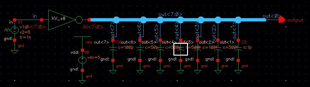
Results
Next
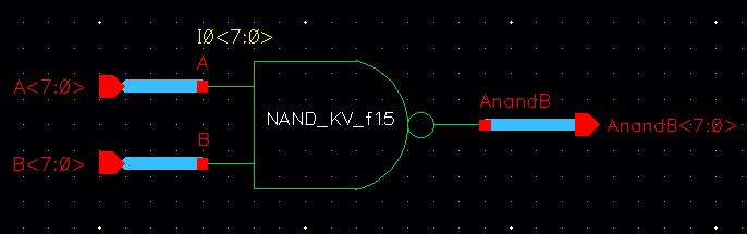
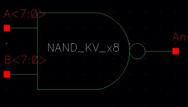
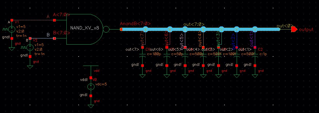
create a nand gate, using a similar process by creating the schematic
and corresponding symbol. Then create an 8 bit nand by using a bus like
before. Lastly we then have to simulate the 8 bit so that we know it
is working properly.
Schematic and symbol (both of which were created in a previous lab).
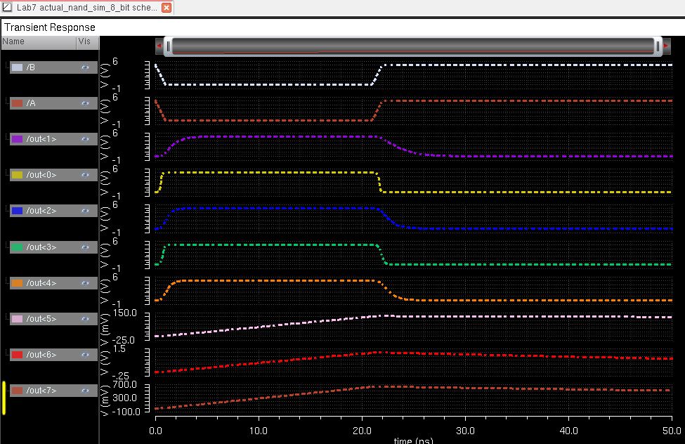
Simulation of 8_bit_nand
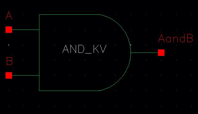
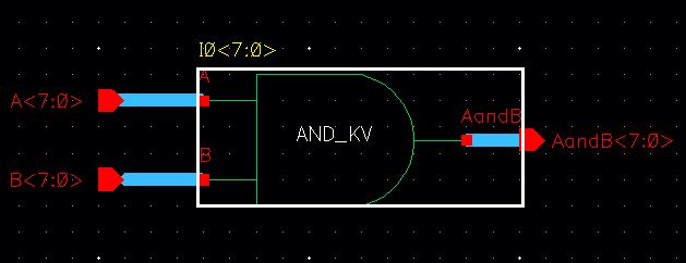
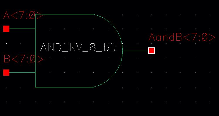
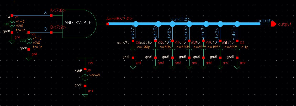
Now to create an 8bit AND gate. This is the same as a nand gate but with an inverter tied to the output.
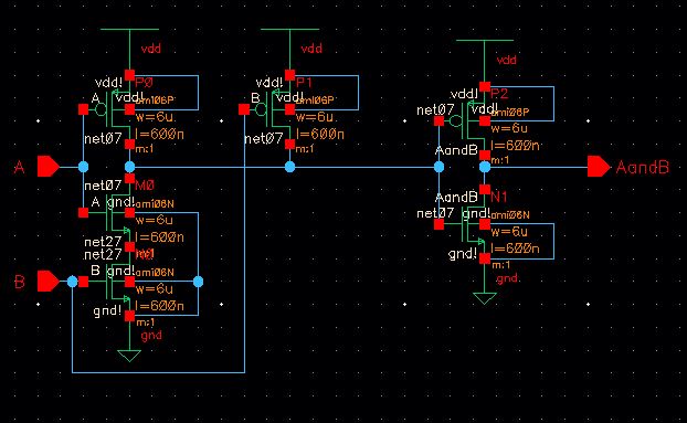
Symbol
8bit schematic & symbol
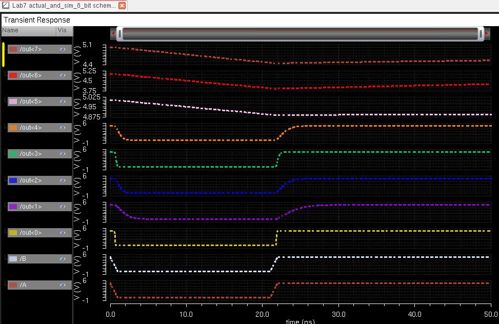
Simulation schematic & results using different capactive loads.
Results
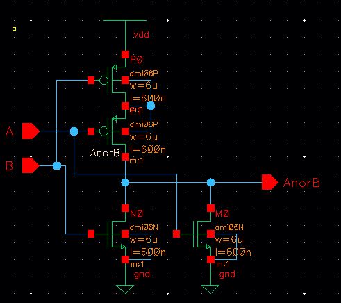
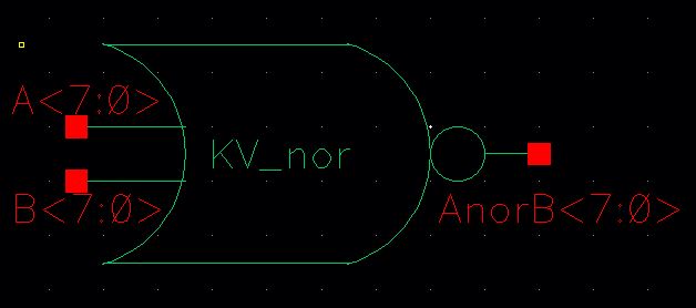
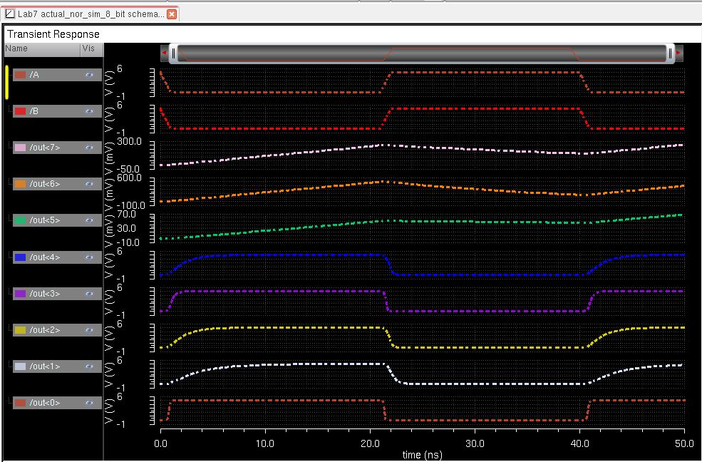
Now to repeat the process but creating a nor & an 8-bit nor.
Schematic
8 bit schematic using symbol created from 1 bit schematic
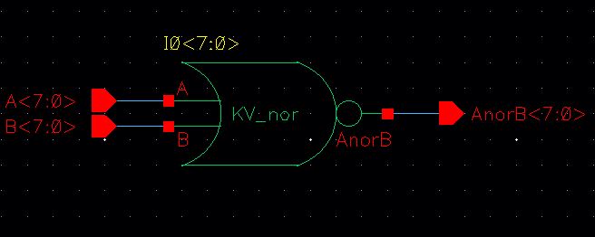
8 bit symbol
simulation
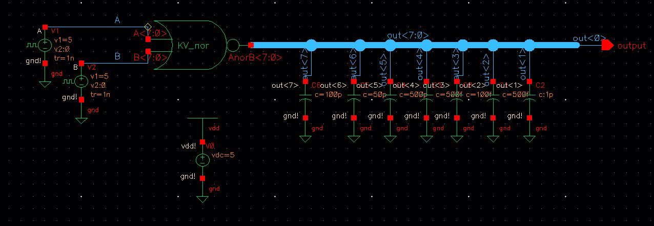
Results
next
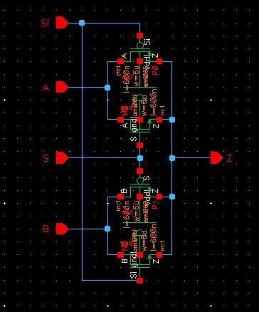
we need to create the same procedure as above but for a mux.
First we had to create an 8 bit mux inculding the si feature and
then an 8bit mux without the si pin and using the inverter int he
schematic.First we will do the regular mux schematic:
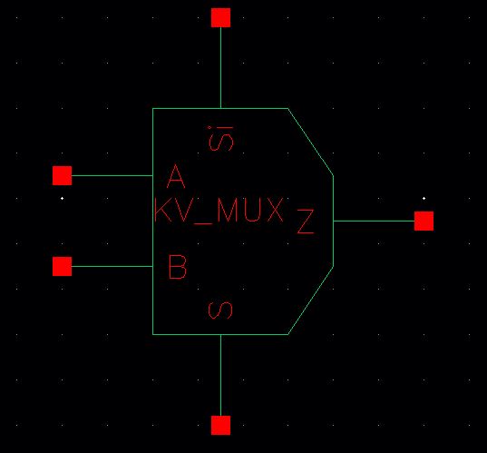
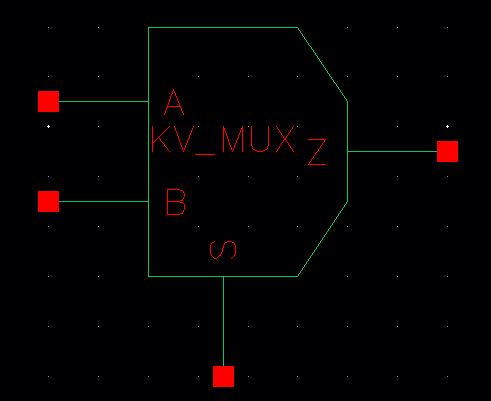
Mux Symbol
As you can see above it has SI in it and we want to create one without SI also:
In order to do this, put the inverter from s to si instead of having it as a sepearte pin in the schematic.
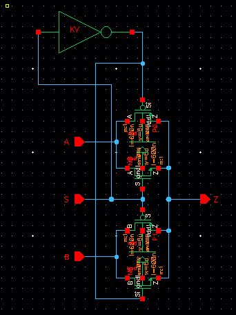
Corresponding symbol
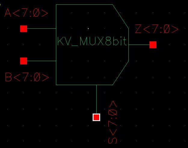
Now to create an 8-bit mux schematic.
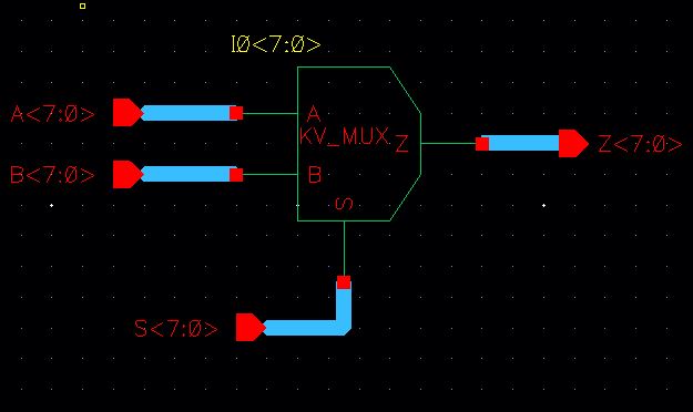
Corresponding symbol
Now to test the mux schematic to verify it is working properly
This is the simulation schematic
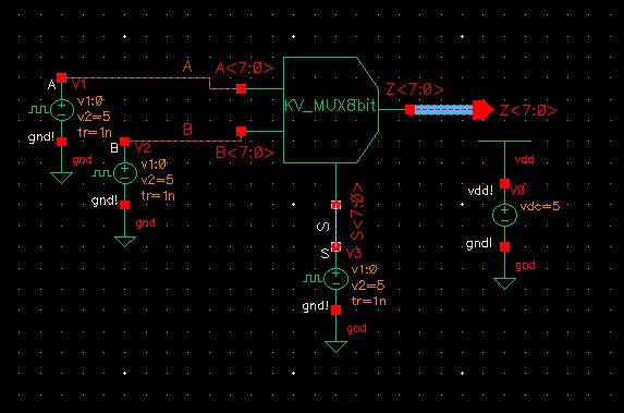
Simulation results
Now
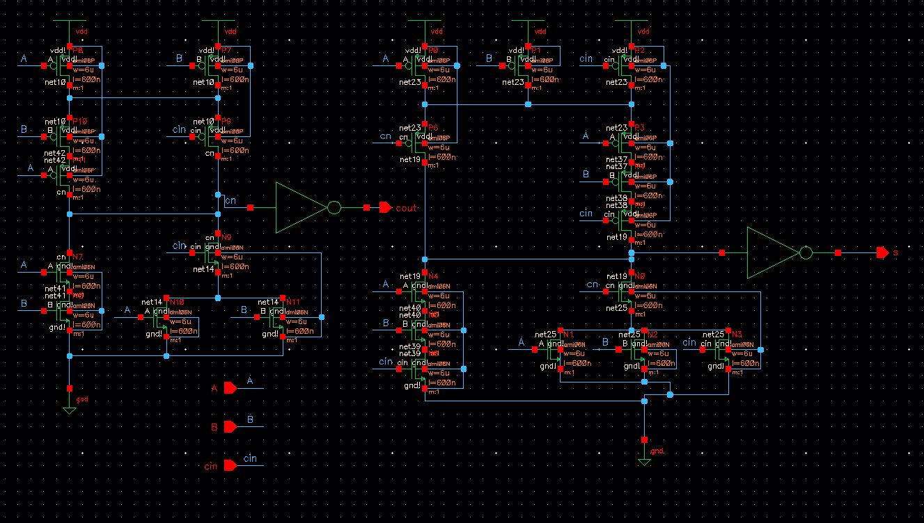
we move on the the last part of the lab 7 the FA. This full adder is
different from the one in the last lab so make sure you dont just copy
the layout and schematic. This is from Prof. Bakers book fig.12.20.Now
to create a 1 bit FA & symbol so we can create an 8 bit FA. Then
layout a 1 bit FA & instantiate it until you have 8 bits in your
layout.
FA schematic
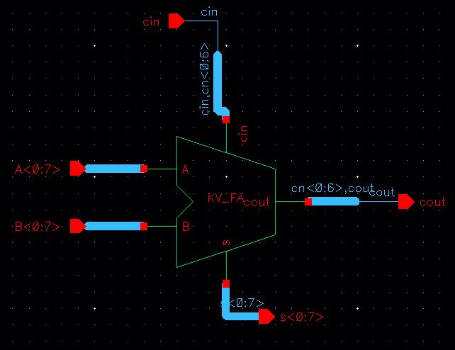
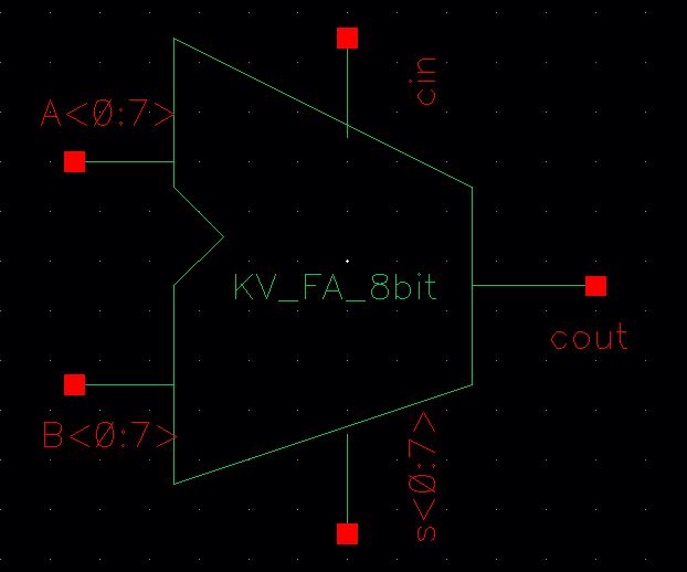
The following are my 8-bit schematic & 8-bit symbol.
Symbol
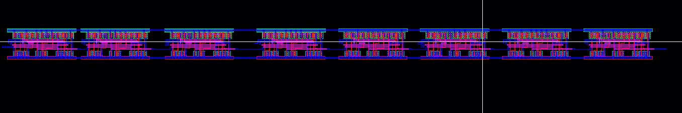
Layout of 8 bit full Adder
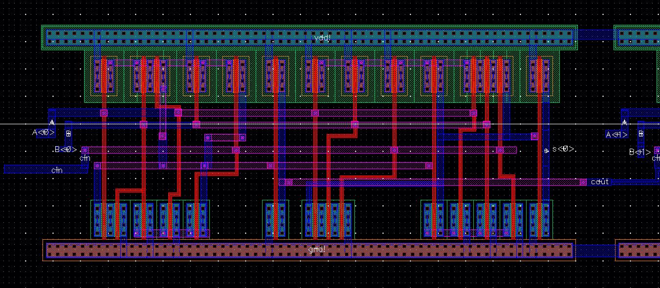
This
is the full adder (1-bit) layout zoomed in.
Note: Label each a and b
pin as input from <0>-<7>. This is the same for the s pins
but as output pins. Also remeber to create 1 cin pin in the begining
and 1 cout pin at the end to match your schematic. Lastly create a pin
of vdd! and ground over all 8 parts of the FA.
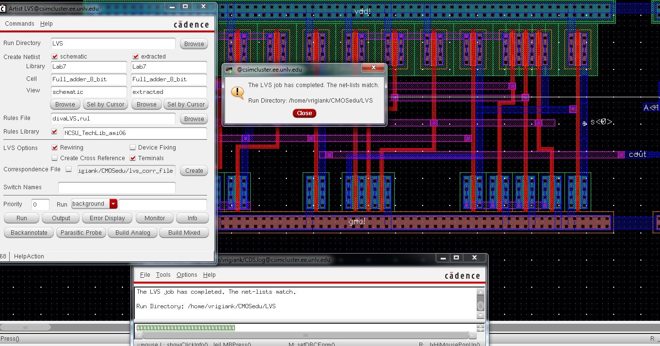
LVS & DRC of layout
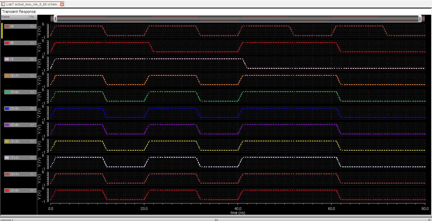
Lastly to test the operation of the 8 bit FA to verify it is working properly.Simulation schematic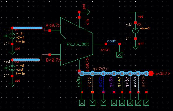
Results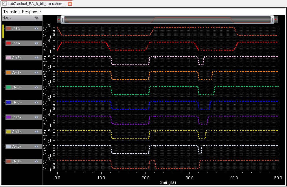
All of the files for this lab can be found here.
Be sure to backup all your lab by uploading it to a drive or online.
Return to EE 421L Labs