Lab 6 - EE 421L
Vrigiank@unlv.nevada.edu
Kirk Vrigian
10/10/15
In this lab we will learn how to create a NAND gate, XOR gate and a full adder using these two gates.
We are using 6u/600u NMOS and PMOS for these gates.
2-input NAND gate schematic.
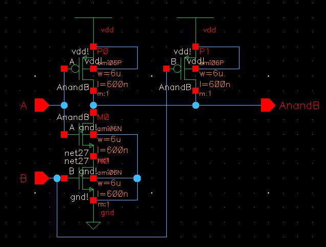
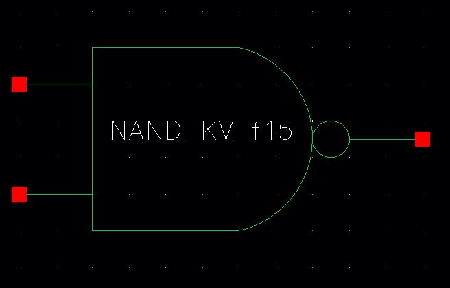
Using this schematic, we crate a nand symbol.
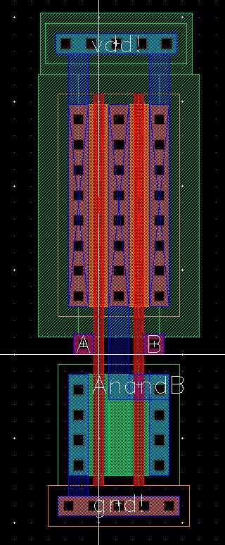
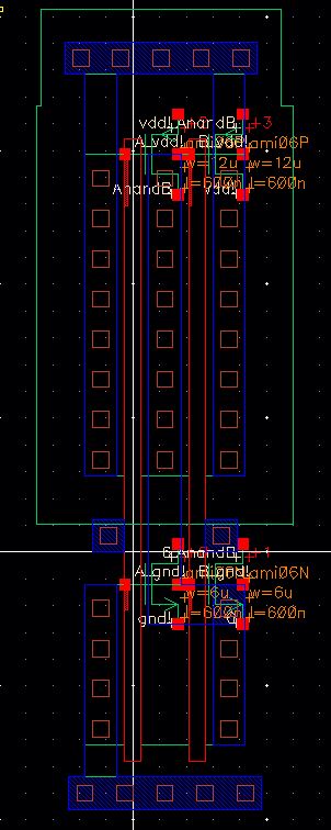
The
layout of our NAND gate, connecting the two NMOS & PMOS by
overlapping the gate of the PMOS & NMOS. Then deleting the center
metal 1 rail in the pmos, flattening them and not preserving pins.
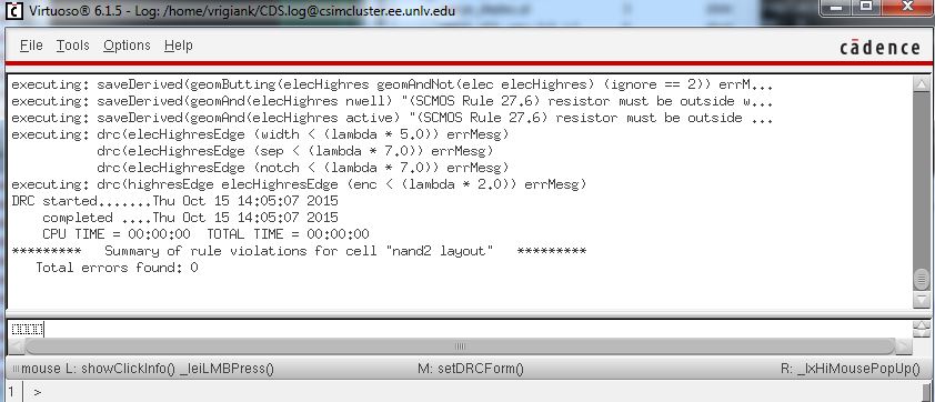
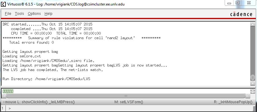
DRC
Extracted view
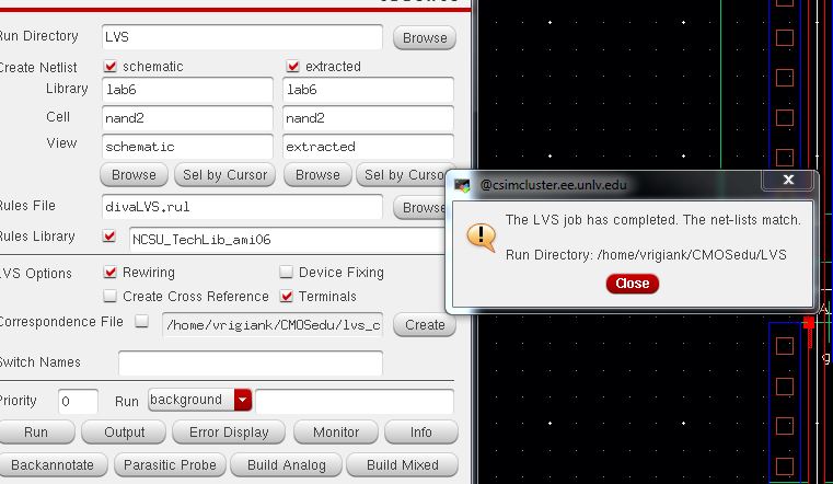
LVS
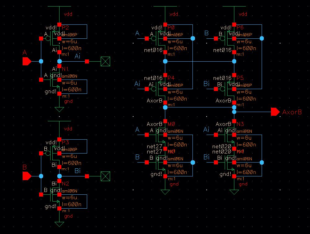
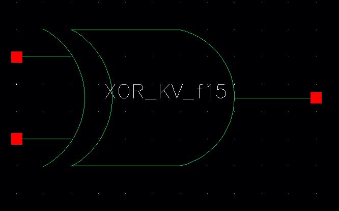
Our XOR gate schematic
Create a symbol from the schematic
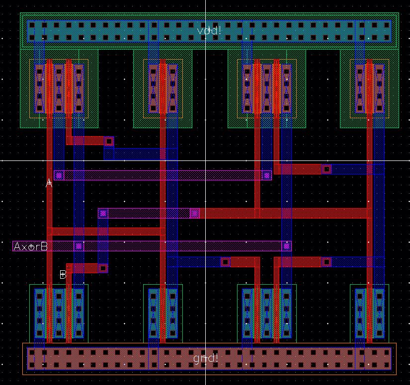
Layout of the XOR gate.
Due
to the complexity of the XOR gate, I used metal 2 to bridge some of the
connections. This was done using m2_m1 & m1_poly contacts.
DRC layout and ensure no errors.
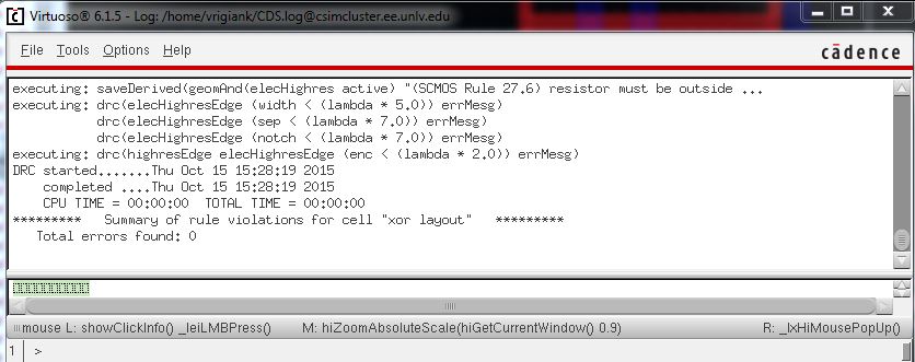
Extracted view of XOR gate.
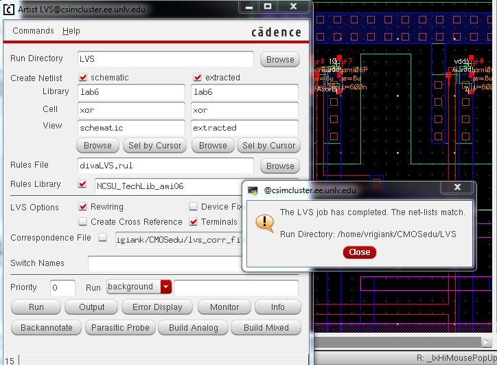
LVS of extracted layout
Now to simulate the NAND & XOR gates.
We will use a schematic utilizing the NAND, XOR, & the 12u/6u inverter from the previous lab.
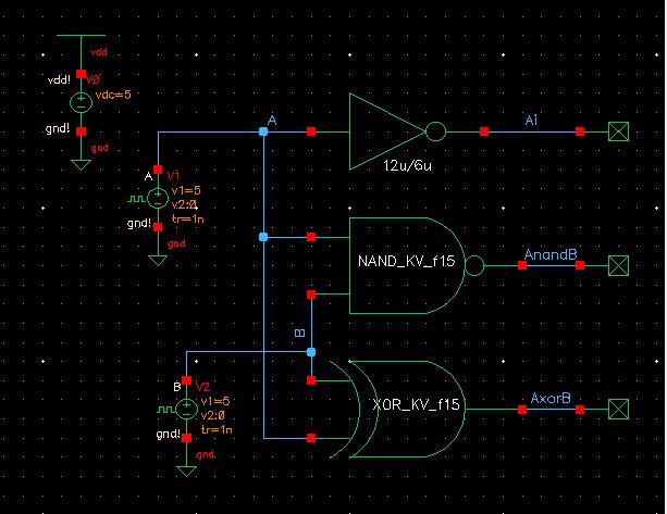
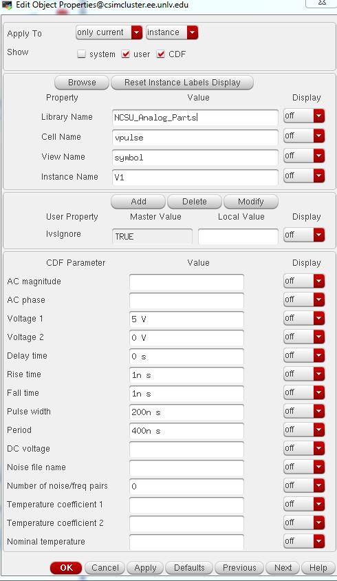
For our pulse sources, A input will use these settings.
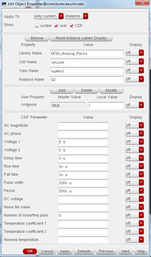
Input source B, will use these pulse settings, with one half the pulse width & period.
Launch ADE L & simulate the schematic using a .tran of 400n.
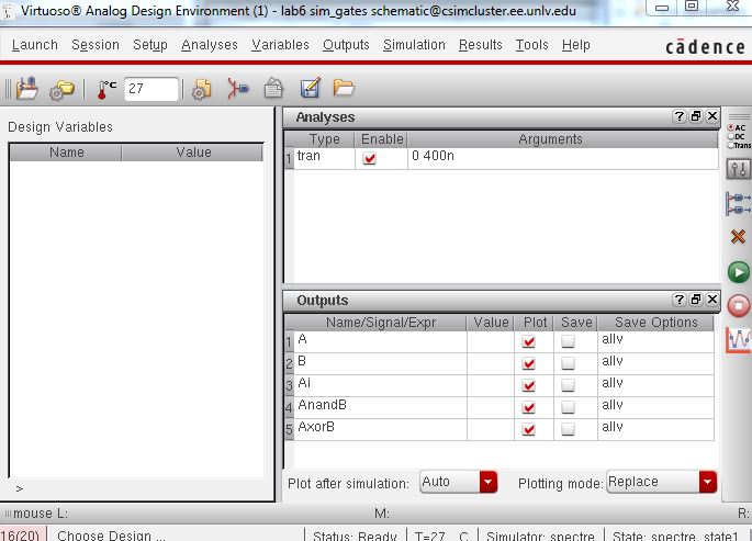
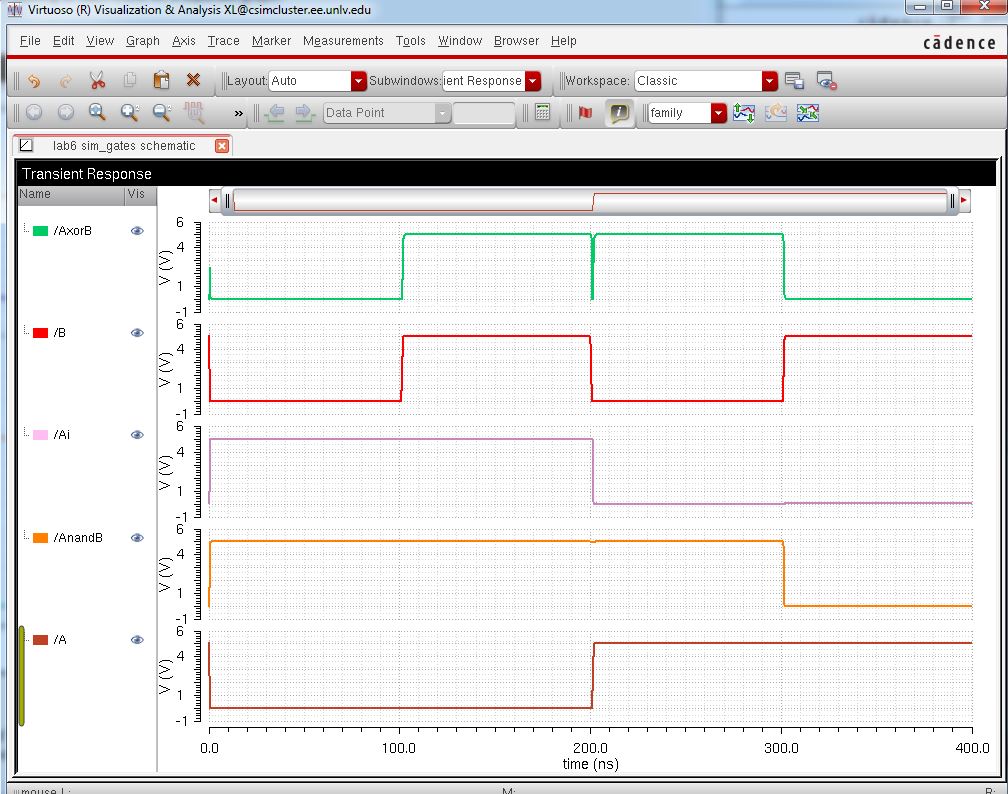
Which should result in the following.
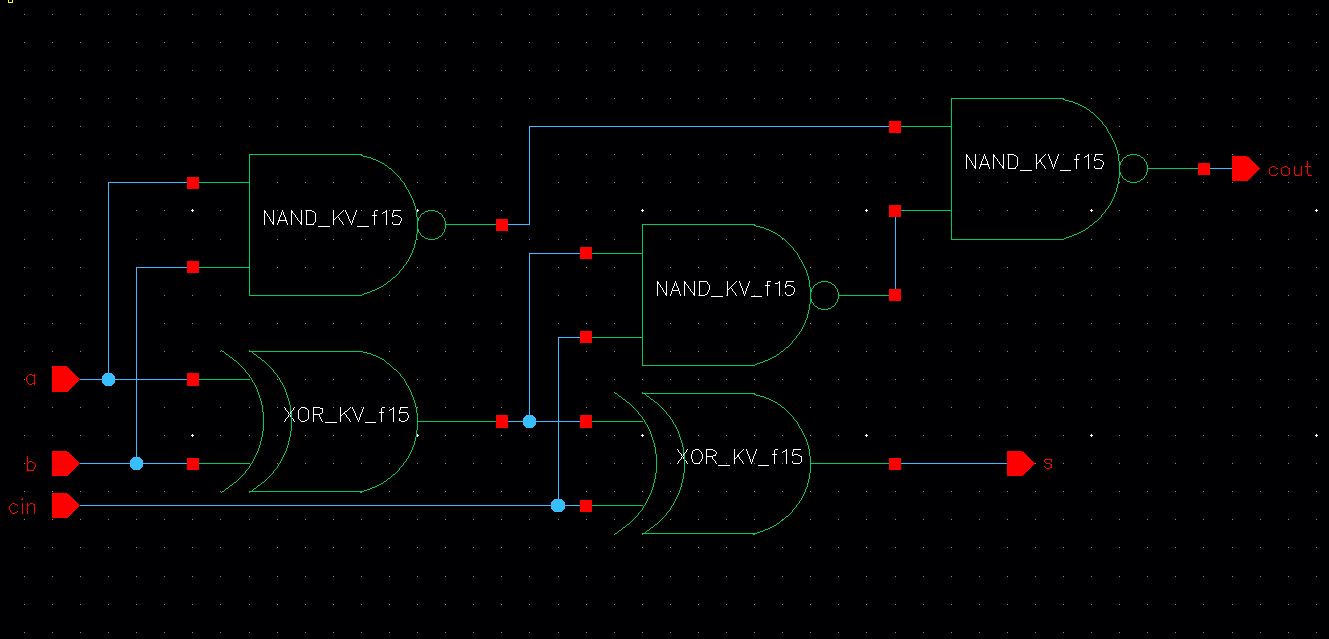
Now to create a full adder using the NAND & XOR gates.
Full adder schematic below.
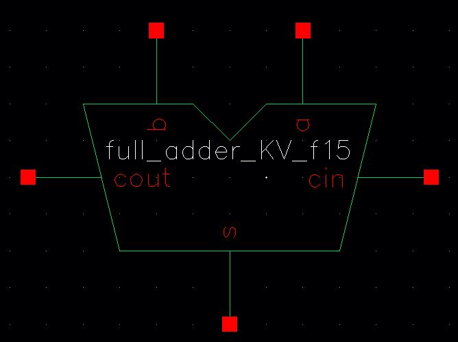
Create a symbol of the schematic.
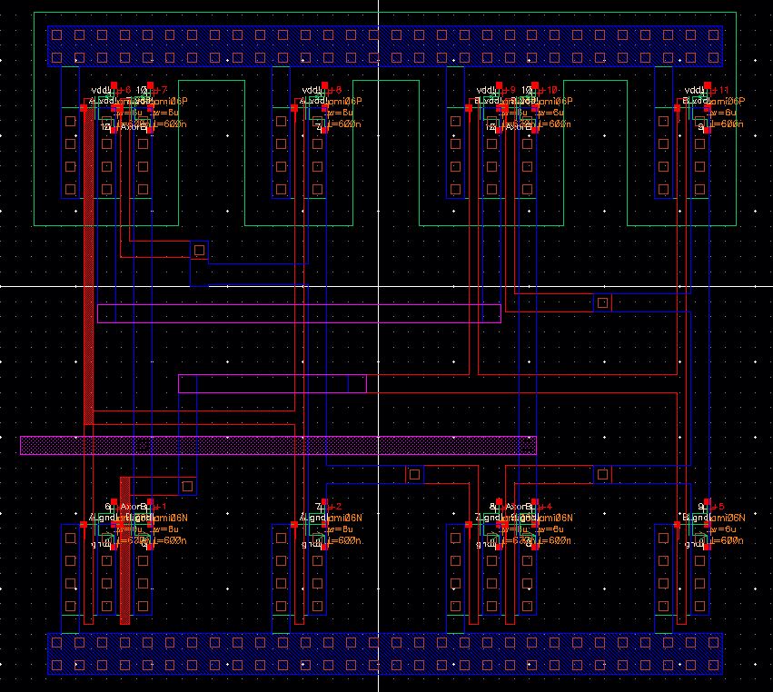
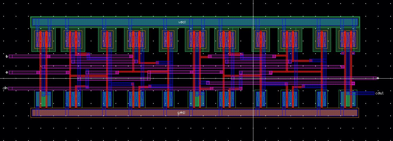
The
layout of the full adder. This was accomplished using three NAND gates
& two XOR gates. To create this layout, instantiate the layout
views of the NAND and XOR gates. Using
the flatten option in the Edit -> Heirarchy -> Flatten, allows
the user to stretch the NAND gate and XOR gate enough to allow for
more
connections for the adder. Also connect the vdd! and the gnd! connections of the MOSFETS into a big row of ntaps and ptaps.
The inputs are the on the left & the output/cout are on the right.
Ensure the layout DRC's
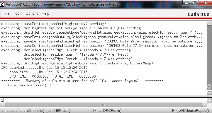
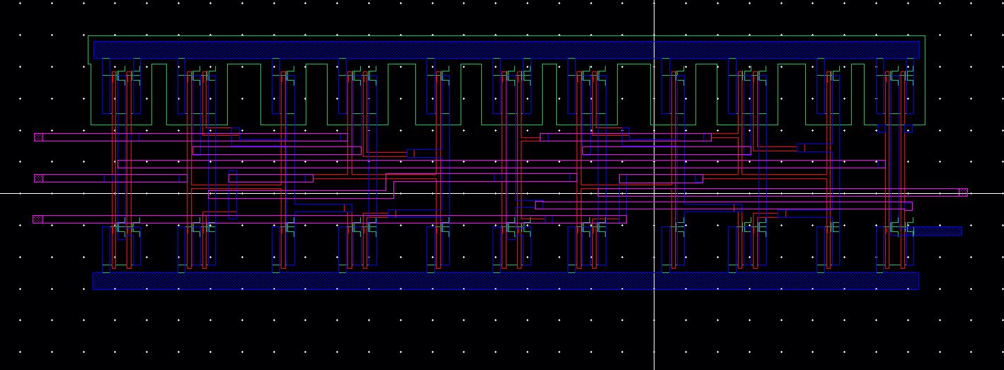
The extracted view of the full adder.
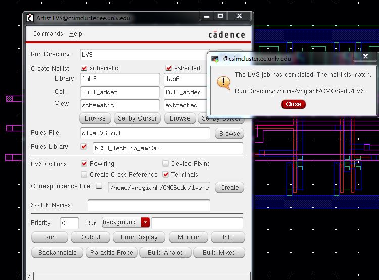
LVS the extracted vs. the schematic.
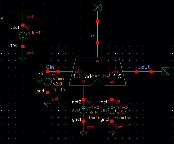
Now
to simulate the symbol created for the full adder, simulate in a
similar fashion to the NAND & XOR gate schematic. Create a
schematic using the symbol & attaching the same A & B pulse
sources, but also include the Cin pulse source. Cin will be 1/2 the
pulse width/period of B & 1/4 the pulse width/period of A.
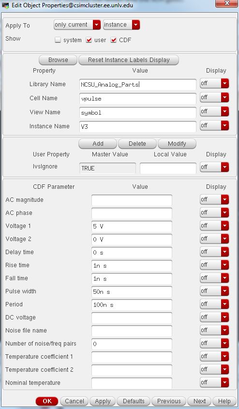
Cin pulse settings.
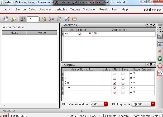
Open ADE L & simulate the adder by running a .tran at 400n again.
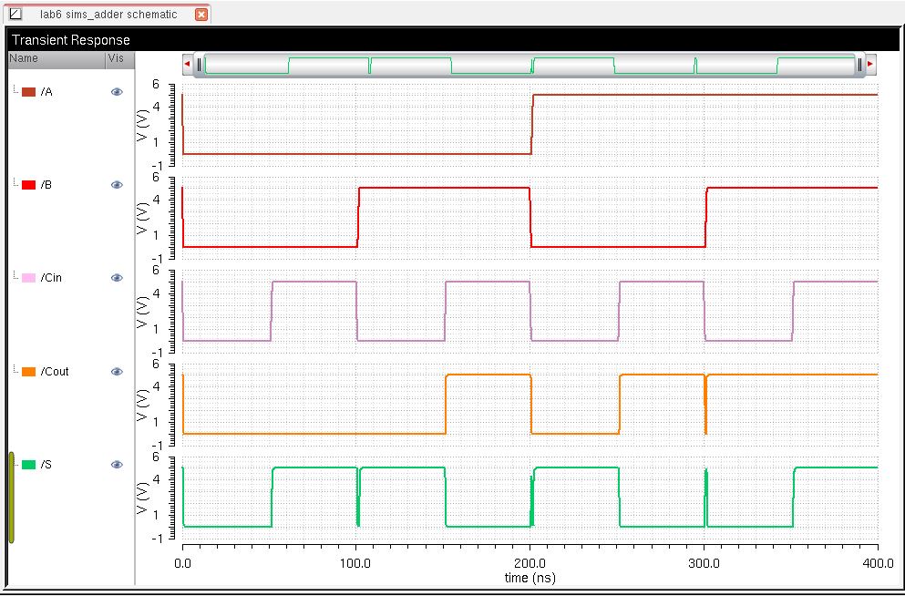
The following results will occur (with split traces).
All of the files for this lab can be found here.
Be sure to backup all your lab by uploading it to a drive or online.
Return to EE 421L Labs