Lab 5 - EE 421L
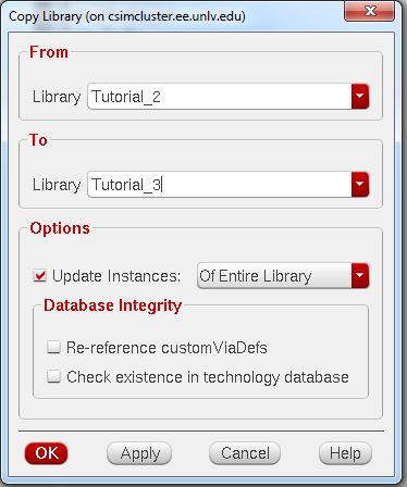
First, we copy tutorial_2 to a library named Tutorial_3, and update instances of library.
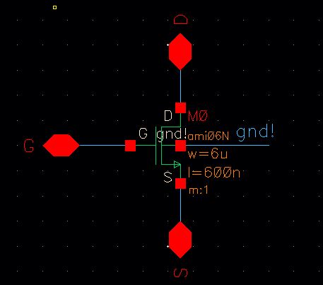
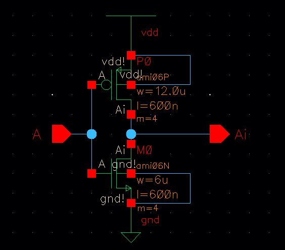
Copy the NMOS schematic over to the inverter schematic by typing C and left clicking the NMOS_IV schematic & drag it over to the inverter schematic.
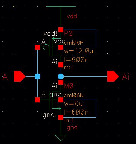
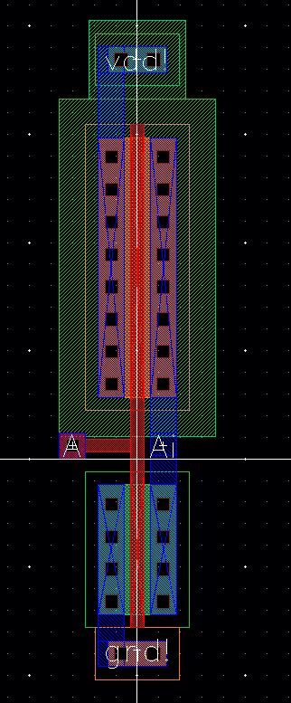
Add the four appropriate pins, draw metal 1, poly rectangles & connect them in a fashion to follow the pin connections for vdd!, gnd!, A, & Ai
Layout of inverter.
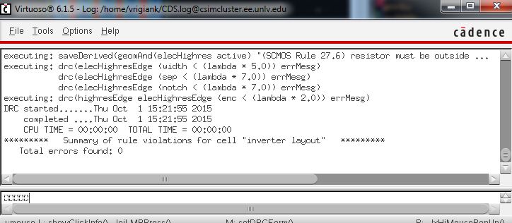
DRC & save your layout, then extract your layout.
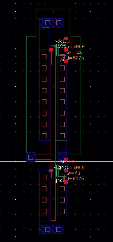
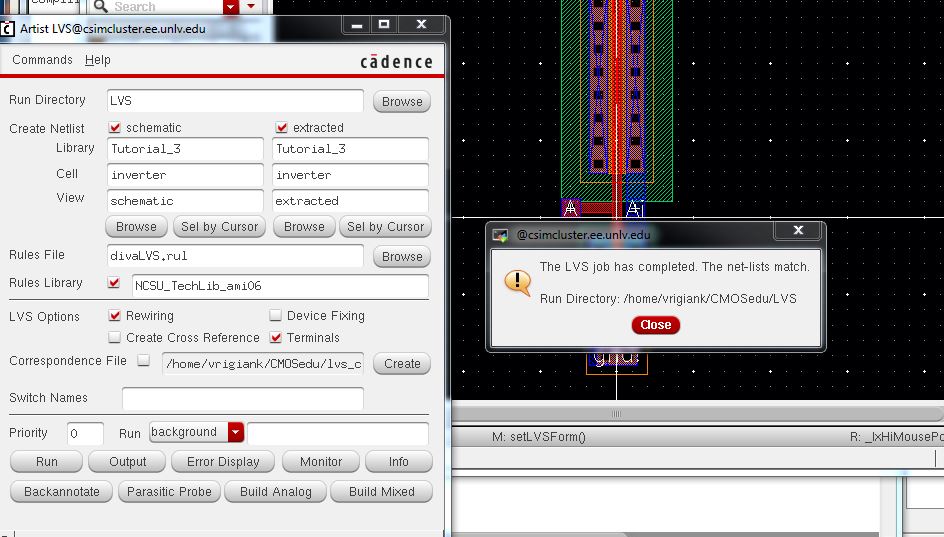
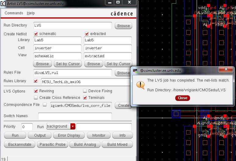
LVS your extracted with schematic.
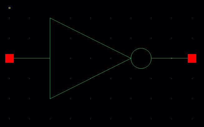
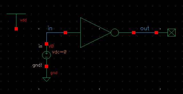
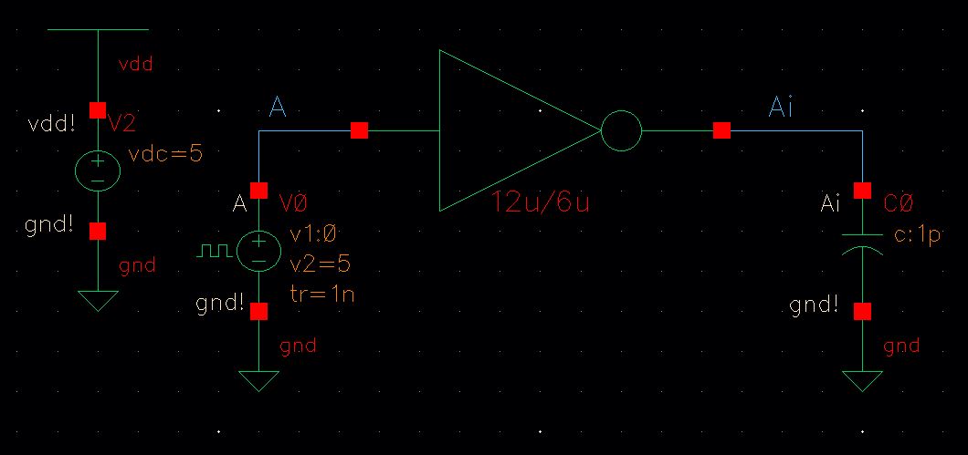
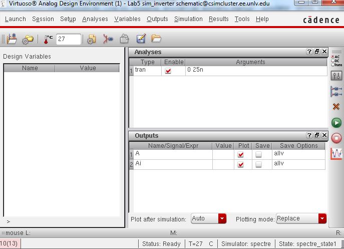
Now let's simulate our inverter. Create a new schematic cell view called sim_inverter_dc. Draw the following schematic seen below, the symbol on the right is the no-connection symbol (basic library, Misc -> noConn), this will help us from getting an error on the floating point.
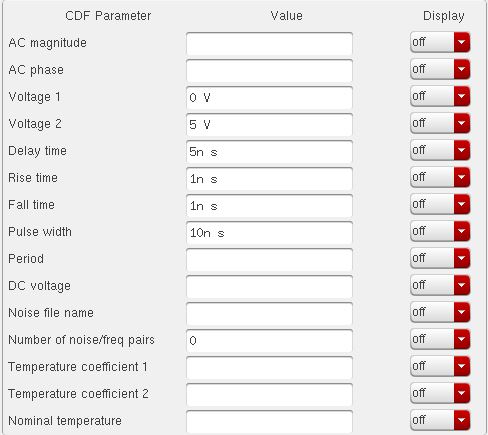
Launch ADE L & select the corresponding models, this would be our ami06p.m & our ami06N.m models. Then select DC analysis with a 1 mv step size, from 0v-5v, and plot in & out. NOTE: before you simulate you need to establish what your VDD! is. Do this by going to setup -> stimuli & click global sources, click vdd!, enable it & set the voltage to DC 5v, source type dc.
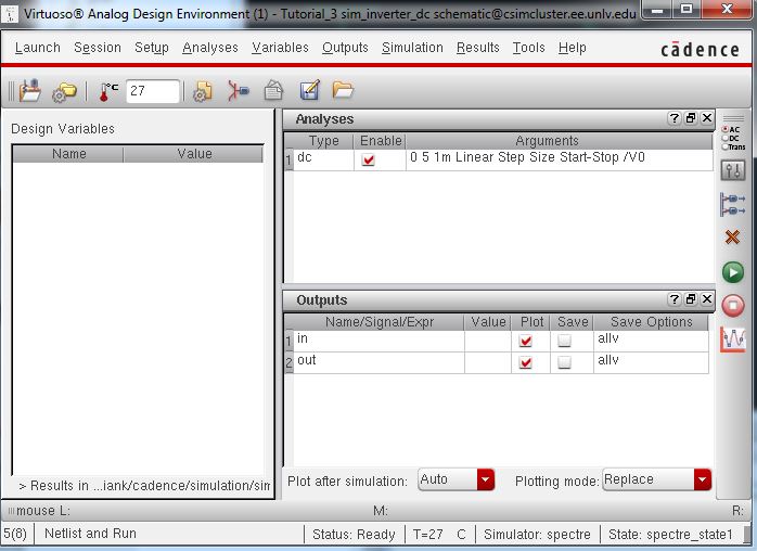
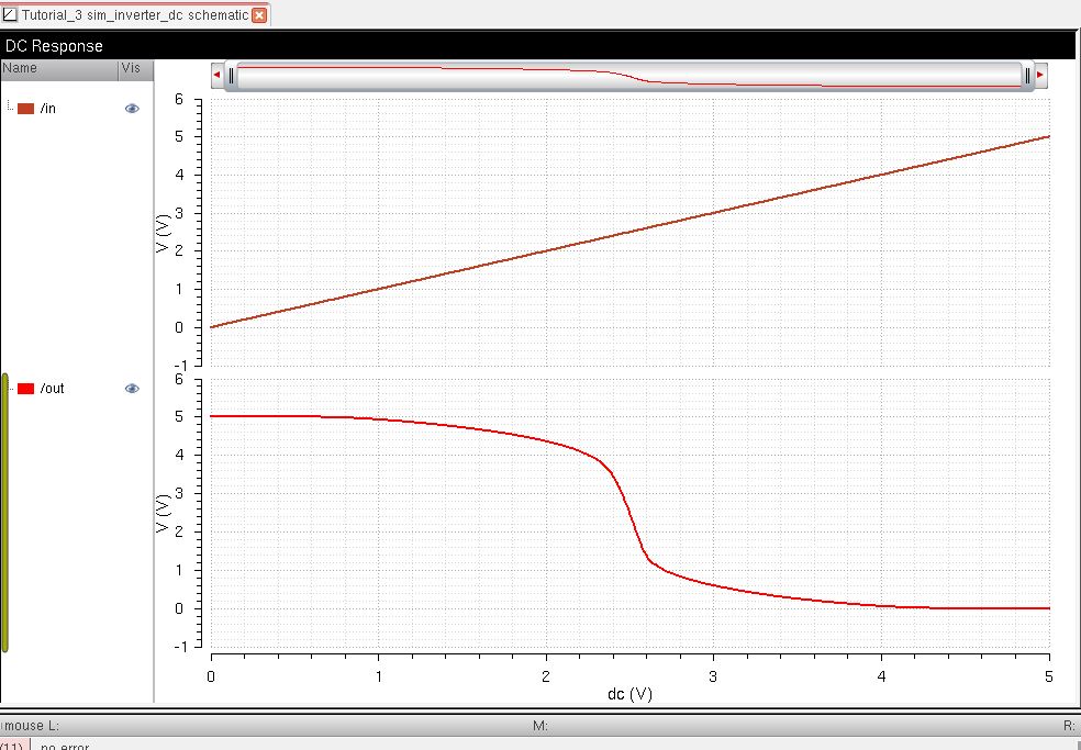
Save the state in cell view & run the dc analysis. Click split current strip & click trace and you will get the following.
Now simulate the extracted layout by going to Setup ->Environment and add 'extracted' in front of the term 'schematic'. You will get the same results (assuming you drew the layout correctly.)
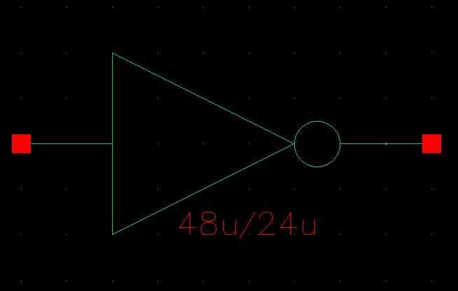
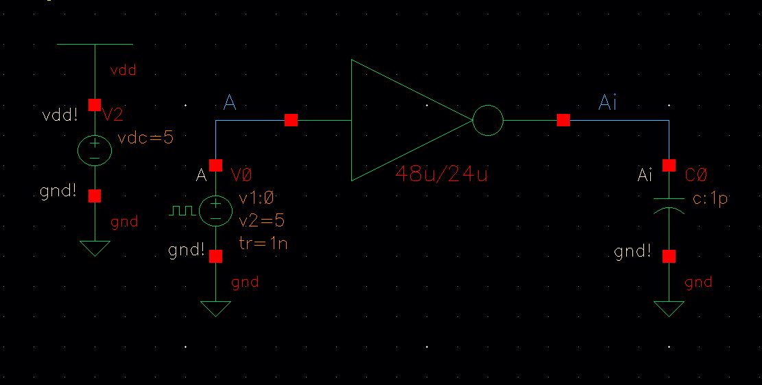
Next we'll create a 48u/24u inverter. First copy over your 12u/6u inverter cell view into inverter_48u_24u. Open the schematic view & edit the properties of both your NMOS & PMOS. Change your multiplier value (m) to 4.
Create a symbol from cellview & repeat the process like earlier. This time we label it with a note, 48u/24u.
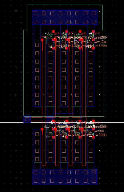
Check & save, then close your symbol. Now Open your copied layout of your 12u/6u inverter. Change the multiplier to 4 for your NMOS & PMOS layout. Also increase the side of your ntaps & ptaps. Draw metal_1 & poly rectangles in a similar fashion to the image below to ensure your pins match the connections with the inverter schematic.
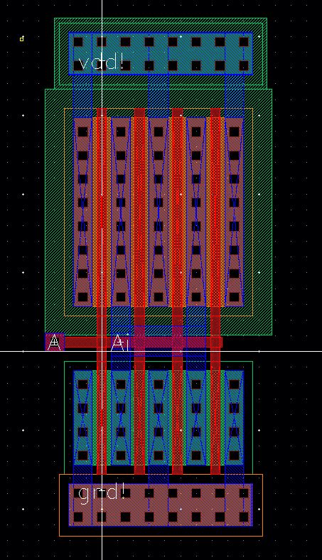
Extract the layout & replace the one you had from the copied cell, it should looks similar to this.
LVS the new extracted layout with the new schematic, it should LVS correctly.
Now to simulate the inverter symbols driving a 1pF, 10pF, 100pF, & 100fF capacitive loads on boath inverters.
This is the 12u/6u inverter.
The 48u/24u inverter
| Inverters | 12u x 6u inverter | 48u x 24u inverter |
| 1 pF load | 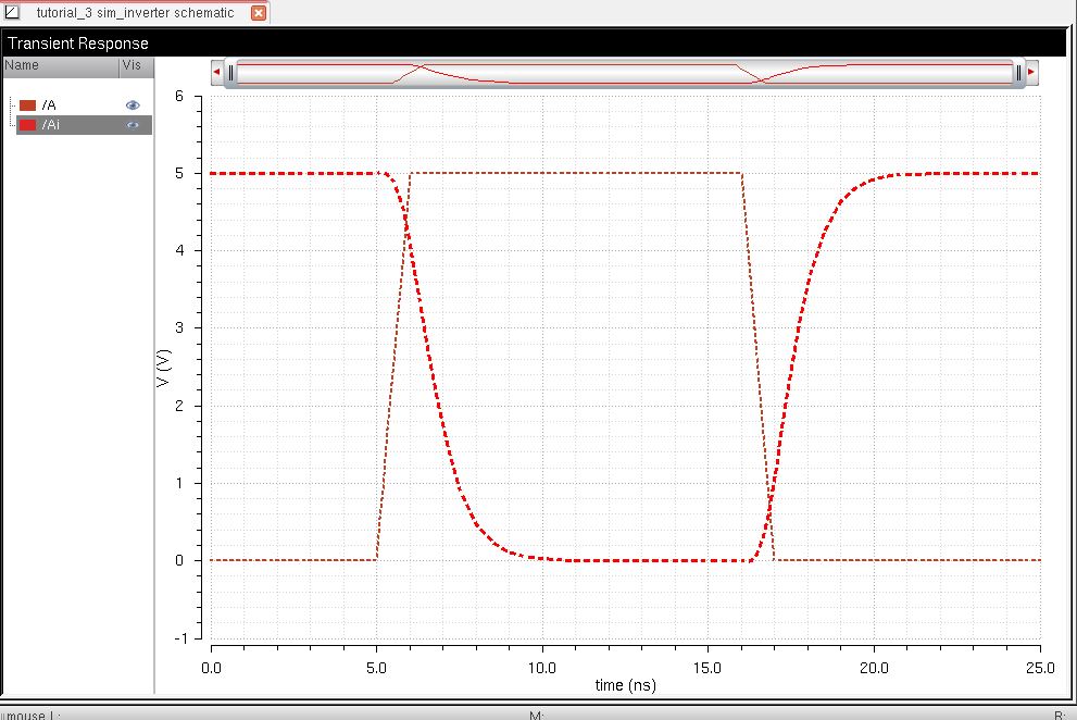 | 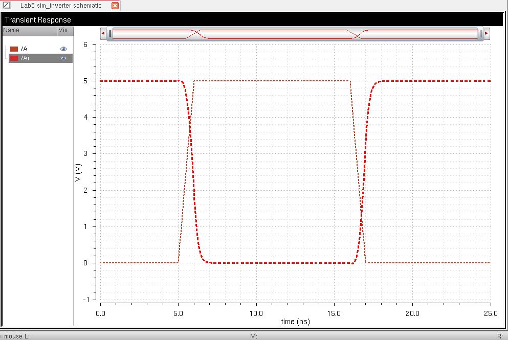 |
| 10 pF load | 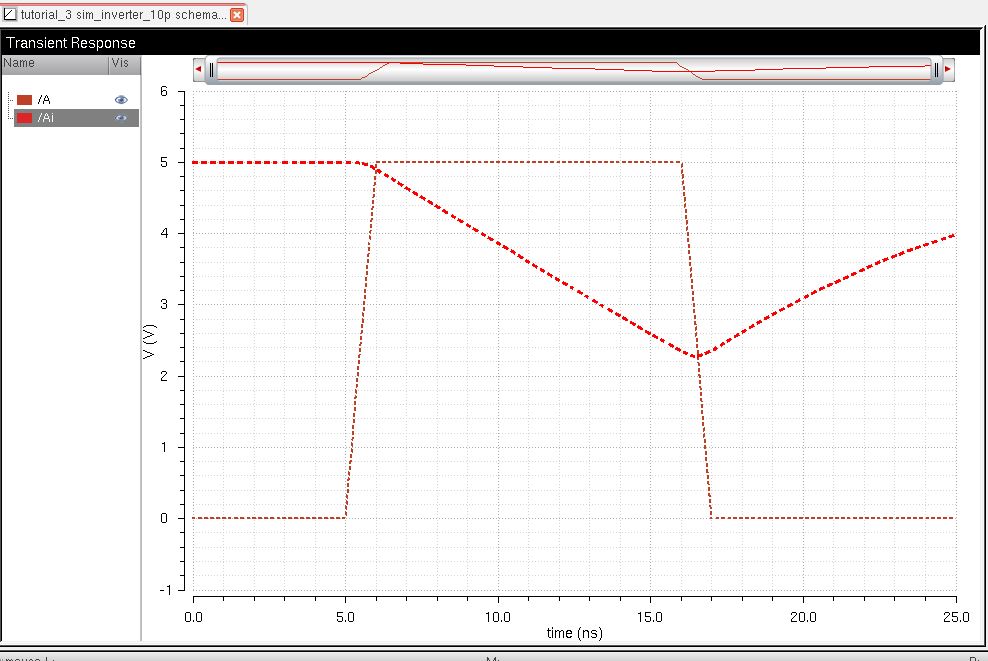 | 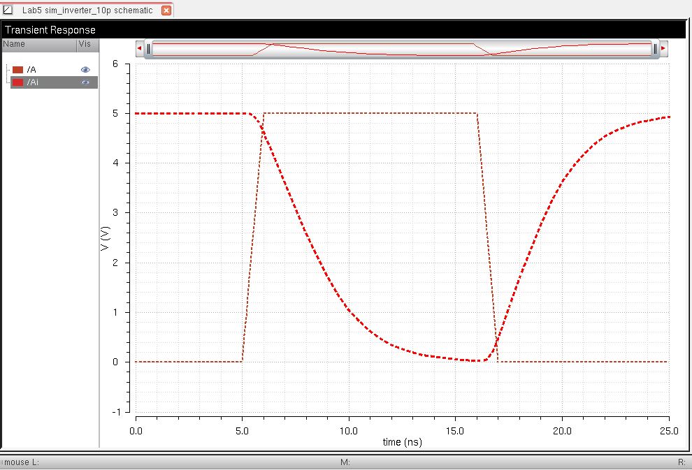 |
| 100 pF load | 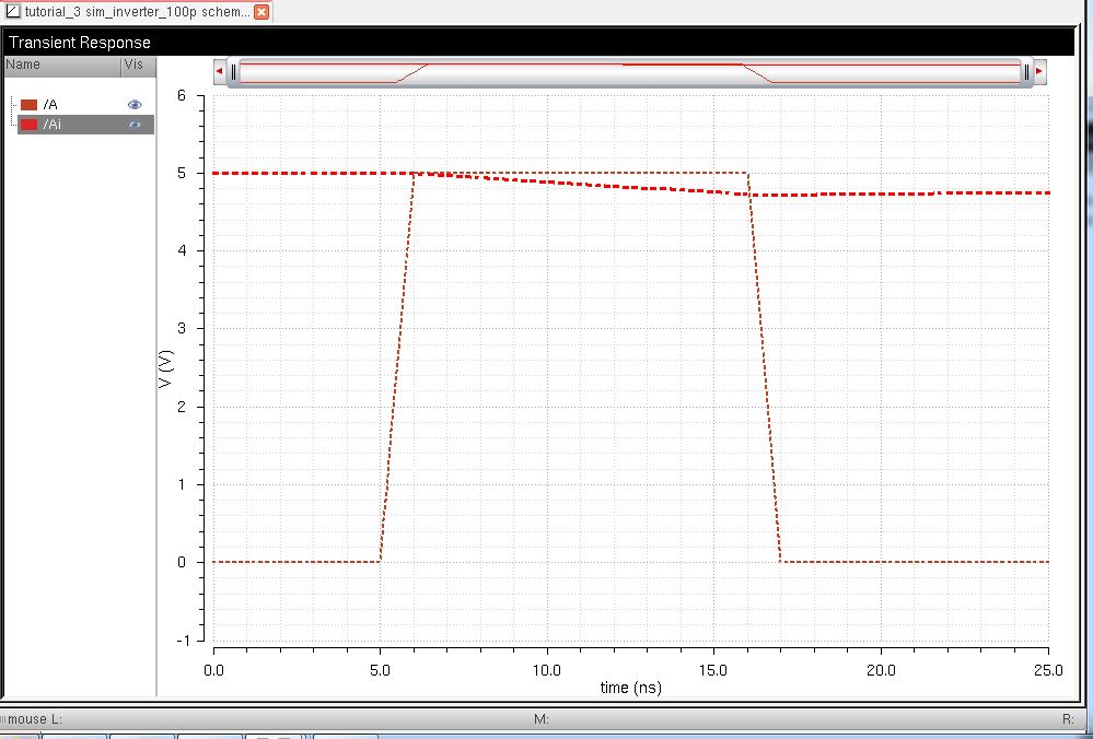 | 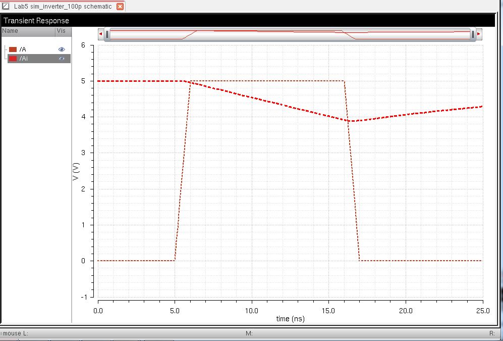 |
| 100 fF load | 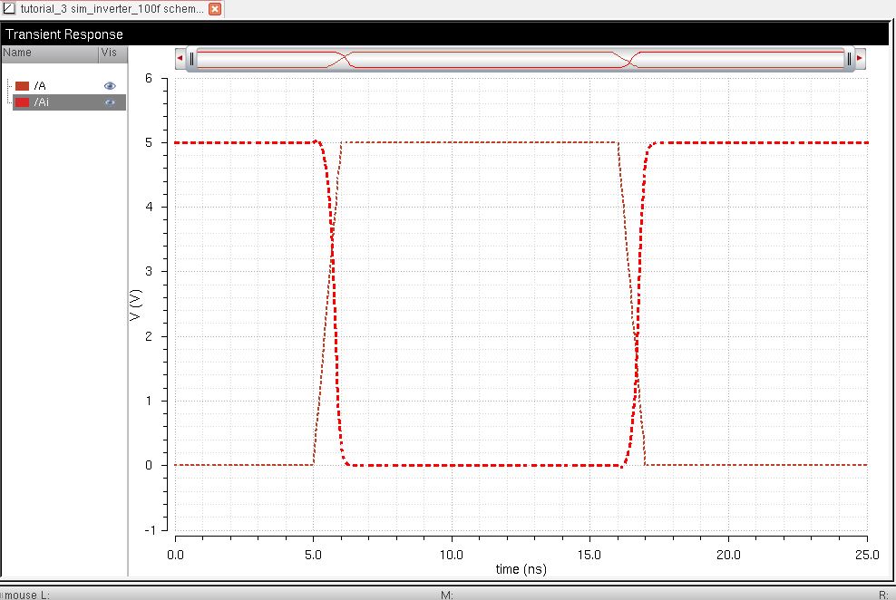 | 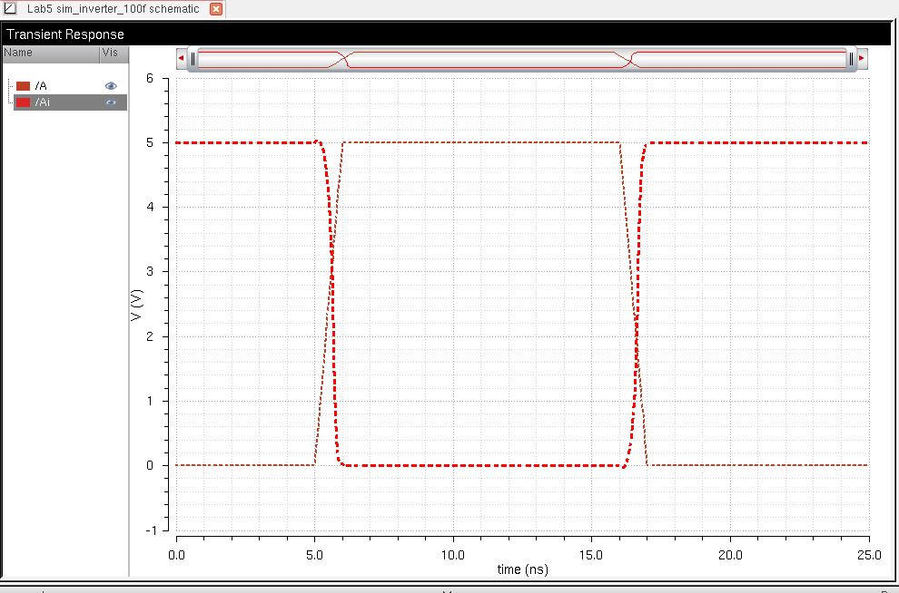 |
The results vary not only by the capacitive load, but for also the two type of inverters. When the capacitor value becomes larger, the more time it takes for it to fully discharge & match the inverse of the input. Which is obvious when you compare a 100pF load vs a 100fF load.
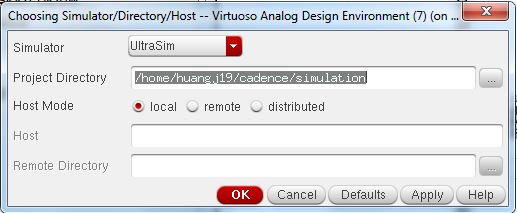
Now we need to re simulate these using UltraSim (which is a fast SPICE simulator for large circuits but sacrifices accuracy & and can only perform transient simulations).
To use this, go to your ADE L window click Setup -> Simulator/Directory/Host. In the simulator drop down window select UltraSim.
| Inverters | 12u x 6u inverter | 48u x 24u inverter |
| 1pF Load | | |
| 10pF Load | | |
| 100pF Load | | |
| 100fF Load | | |