Project - ECE 421L
Authored
by Giang Tran
11/09/2015
trang@unlv.nevada.edu
Part 1: Up/Down Counter
Drafting a counter with synchronous clear.

Counter Symbol

Simulate

Transient Response.
-This is an edge triggered D flip-flip so the output only changes whenever clock goes high.

Drafting our up/down counter with select.

Draft the following to simulate our 8-bit counter

The following is the response of our counter.
When sel is high, the counter counts up. When sel is low, the counter counts down.

Notice
the glitches in the middle. This happens only when the Sel goes from
high to low or low to high. The glitches happen since our counter
cannot instantly switches from up counter to down counter.
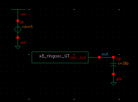
31-stage ring oscillator
Draft the following circuit for a 31-stage ring oscillator with a buffer for driving a 20pF off-chip load.

Symbol of a 31-stage ring oscillator with buffer.

Simulation part
Transient Response

Nand/Nor gates
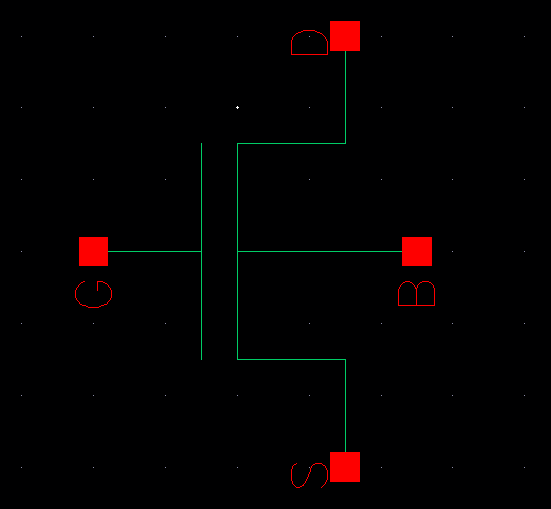
Draft the following circuit for NAND gate

Draft the following circuit for NOR gate
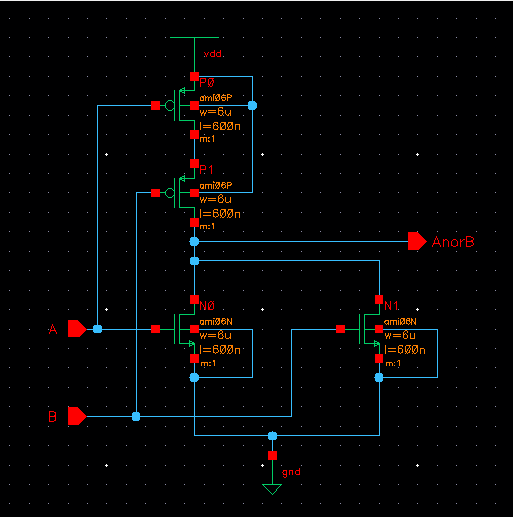
Simulation of our NOR and NAND gates

Inverter
Creating schematic for our inverter
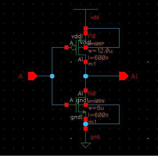
Creating
symbol and run the simulation. We'll get the following transient
response. This is an inverter, hence, whenever input is high, output
will be low.

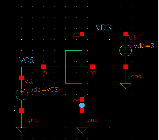
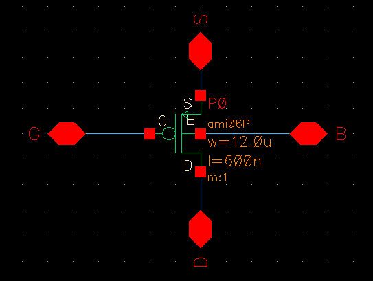
NMOS
Our NMOS will have 4 terminals
-G : Gate
-B : Base
-S : Source
-D : Drain
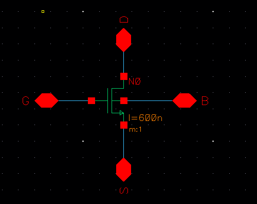
Creating symbol
Draft the following circuit to simulate our transistor.
We'll get the following curve.

PMOS
Pmos will also have 4 terminals: Drain, Source, Gate, and Base
Creating symbol

Simulating
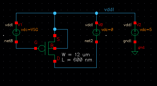
Transient Response

25K and 10K resistorS
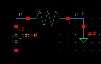
Resistor with inputoutput pins. This is a 25K resistor.
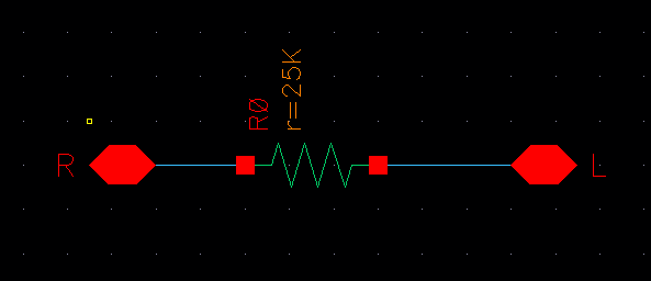
Creating symbol
Simulating
Sweep the voltage source from 0-5V.
We'll get the following linear relationship.

10K resistor schematic
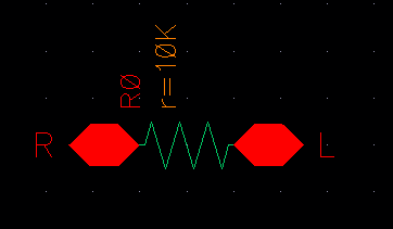
10K resistor symbol

Simulating
We'll get a very similar response.
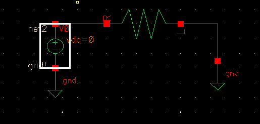
Connect the 25K and 10K resistors together to form a voltage divider.

We'll get the following transient response.
Vout = Vin * (10K / (35K)) = 1.42 V

Project Layouts
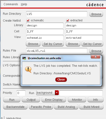
Layout of a D flipflop

DRC check

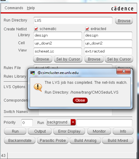
LVS check
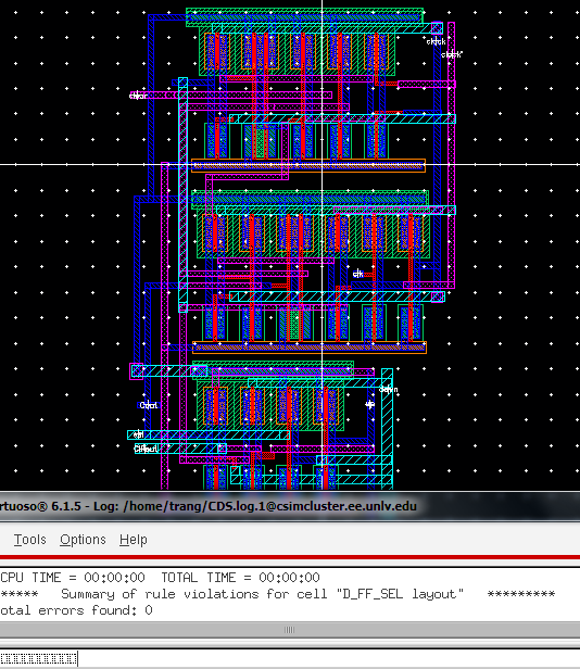
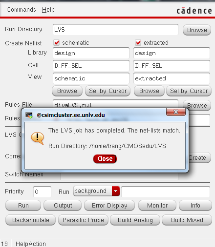
D flipflop with select for counting up or down

DRC check
LVS check
Layout of my up-down counter with DRC check

LVS check
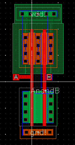
NAND gate layout
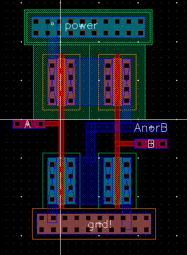
NOR gate layout
I did a quick update to my ring oscillator with a buffer connected to the output.

Ring oscillator layout

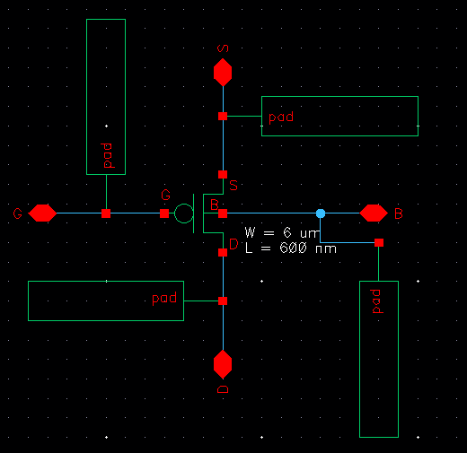
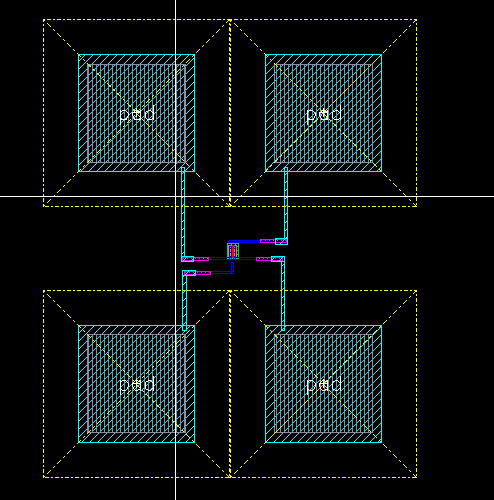
NMOS connected to 4 pads

NMOS layout

PMOS with 4 pads
PMOS layout
Layout of my 10K n-well resistor

Layout of my 25K n-well resistor

Voltage divider layout

Saving My Work!!!
All files and images are backed up in a folder on my desktop,
I'll then send a copy to my email as a backup.
Return to main page here