Lab 7 - ECE 421L
Authored
by Giang Tran
10/28/2015
trang@unlv.nevada.edu
Lab
description:
- Design, layout, and simulation of a ring oscillator.
- Design and simulation of 8 bits AND, NAND, NOR, OR, FULLADDER, INVERTER, MUX.
Pre-Lab
31
stage Ring oscillator is made by placing 31 inverters horizontally with
the final output feeding back into our first input.

We'll get the following waveform

31
stage ring oscillator looks long and complicated if we draft it one by
one. This can be fixed by using an array of 31 inverters.
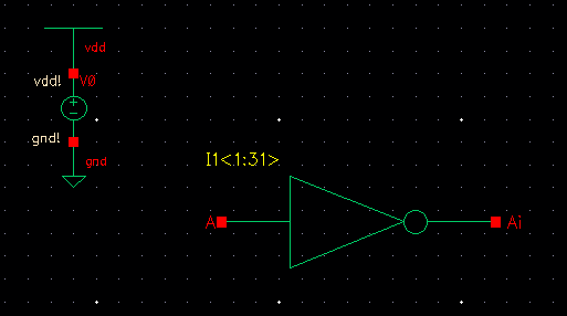
Adding thick wires to input and output.

Add the following labels to input and output nodes.

Check and Save, then run the simulation.

Ring oscillator layout view.

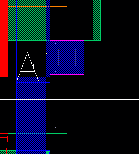
extracted view

layout view

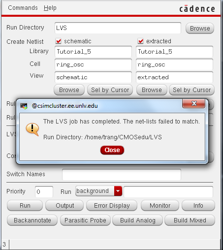
DRC and LVS, LVS fail because we did not create an output pin for our schematic.
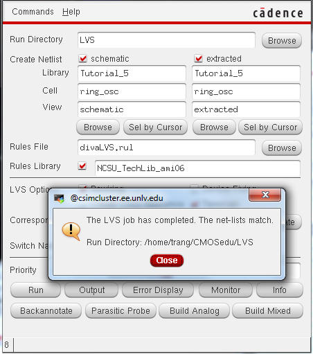
Adding output pin osc_out to schematic.

LVS match!
Create a cellview for our ring oscillator. Then draft the following circuit.

Run the simulation, we should get something very similar to our previous waveforms.

Extracted view simulation


Post-Lab
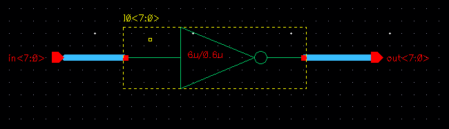
Drafting a 6u/0.6u inverter.

We'll make our 4 bits inverter using the method in our prelab.

Create a symbol for our 4-bit inverter
Simulate our 4-bit inverter driving 3 different size capacitors. Use the following schematic.

Our transient response is as following. We can see that if our input is low then our output is high,

8-bit NAND gate

8-bit NAND gate symbol

Schematic to simulate our 8-bit NAND gate

We'll get the following response

8-bit AND gate can be made easily by adding an inverter to our NAND output.

Creating symbol view

Draft
the following circuit to test our 8-bit AND gate. Note that since NAND
is the inverted version of AND; hence, our output is the opposite of
the previous circuit.

Transient response

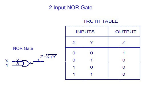
Drafting a NOR circuit

Symbol of our NOR gate.

Drafting our 8-bit NOR gate

8-bit NOR gate symbol

Draft the following circuit to simulate our 8-bit NOR gate

Here's a table for 2 input NOR gate. We'll expect similar response for our output.

To get an OR gate, we'll add an inverter to the output of our XOR gate.

Create a symbol for our circuit.

Drafting a 8-bit OR gate

8-bit OR gate symbol

Draft the following circuit to test our 8-bit OR gate

Transient Response

Drafting a 8-bit inverter
Symbol

Draft the following circuit to test our 8-bit inverter.

Transient Response

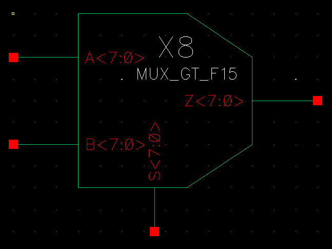
Next up, we'll begin the design of our 2-bit MUX. Draft the following circuit
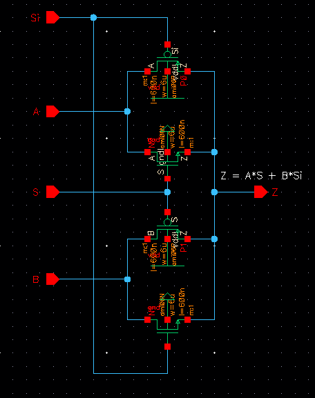
The operation of our MUX is as the following:
-When S is high (1) then Si is low (0)
-The NMOS and PMOS connected to A are turned on causing the output to go to A.
-The PMOS and NMOS connected to B are turned off.
-When S is low (0) then Si is high (1)
-The NMOS and PMOS connected to B are turned on causing the output to go to B.
-The PMOS and NMOS connected to A are turned off.
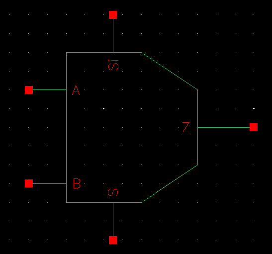
Create a symbol for our circuit.
Sim our MUX to get the following response.

To
create our 8-bit MUX without the inverted S terminal, we'll reuse the
existing schematic of our MUX to speed thing up. We'll connect the S
terminal to the Si terminal through an inverter. That is if S is high
then Si is low (inverted). Note that we'll need a 8-bit inverter for it
to work.

Create a symbol for our 8-bit MUX.
Draft the following circuit to test our 8-bit MUX

Transient Response

Fulladder design

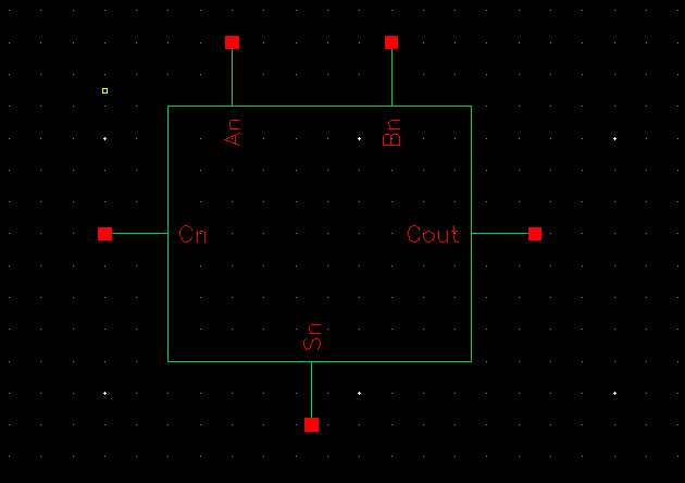
Symbol view
Draft the following schematic to test our fulladder.
Transient Response

Making a 80bit fulladder

8-bit fulladder symbol

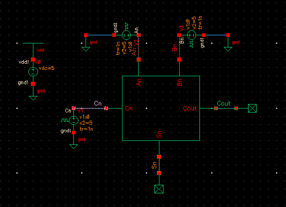
8-bit fulladder testing

We'll get the following response

We'll begin the design of our fulladder. Let's start our with 1-bit fulladder

Make sure there are enough room in between so we can easily connect the wires. DRC and LVS check after finish.

Let us run the simulation again using our extracted layout to verify it matches our schematic response.

Verified!

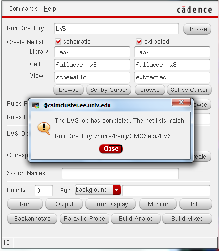
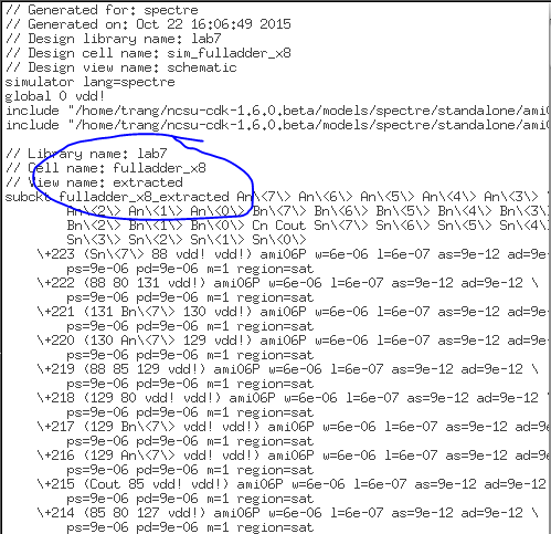
Laying out our 8-bit fulladder

LVS match!
Here's how I connect my 8-bit fulladder bit-by-bit. At the first bit:

At the last bit:

Run our simulation again using our extracted view.

It is verified that we obtain similar result using our extracted view.
I've
used 6 different capacitor values in very single one of our 8-bit
simulations with noticeable differences. The smallest capacitor will
gives us the near perfect output, while the largest capacitor barely
able to discharge. This is because the time delay for the lower value
capacitors is low since T(delay) = 0.7*R*C, hence, small C results in
small time delay. We can keep it simple by treating the capacitors as
buckets. Smaller buckets require less time to fill and empty. While the
bigger buckets require more time to fill and empty. Our 1nF capacitor
sometimes did not have to enough time to discharge then the next cycle
kicks in and fill it back up.
Saving My Work!!!
All files and images are backed up in a folder on my desktop,
I'll then send a copy to my email as a backup.
Return to main page here