Lab 6 - ECE 421L
Authored
by Giang Tran
10/04/2015
trang@unlv.nevada.edu
Lab
description:
-Design, layout, and simulation of a CMOS inverter.
Pre-Lab
-First, we'll copy the library, Tutorial_3, into a new library and name it Tutorial_4. Remember to update instances.
-Copy the inverter cell into a new cell call nand2.
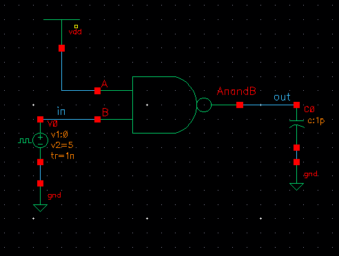
-Open up the nand2 cell, we'll draft the following schematic. This is easier if we use bindkey c and copy the PMOS and VDD.

-Check and Save our schematic, make sure there's no error.
-Proceed to make our symbol of the circuit.

-Make a new cell call sim_nand2.
-Draft the following circuit.
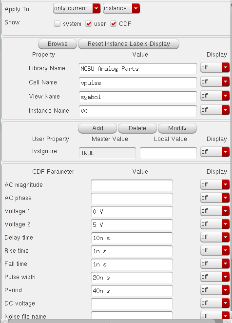
-The properties of our vpulse is as follow.
-Check and Save our circuit, run ADE.
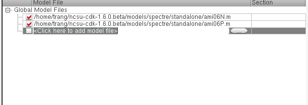
-Set models like below
Run the simulation, we will get the following waveform

Next up, open the layout cellview for our inverter. We'll make some adjustments to the layout.
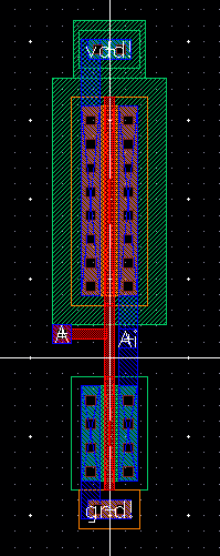
Delete metal1 contacts and ground pin on our inverter.
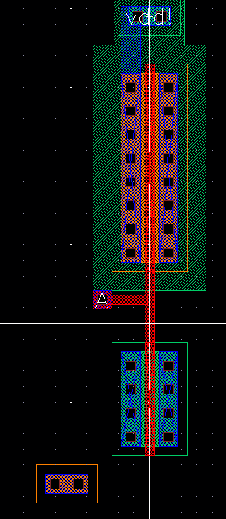
-Copy our PMOS

-Line up the PMOS so that they're overlapping. Expand our ntap cell and align them up like below.

-Do the same for our NMOS and ptap. Create pins for vdd!, gnd!, B and AnandB.

-DRC check our layout.
-Extract layout when finish.

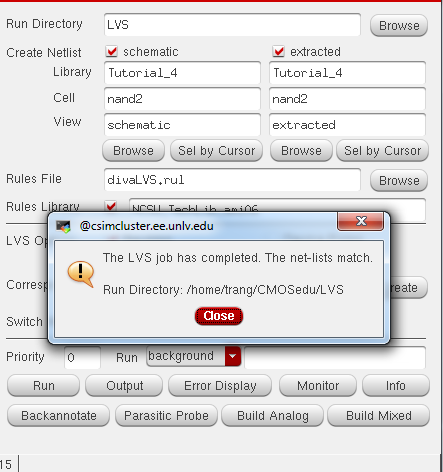
-LVS check our schematic and extracted view. Make sure net-list match!
Post-Lab
-We'll create another nand gate using 6u/600n PMOS instead of 12u/600n in our prelab. DRC check our schematic as always.

-Create cellview from schematic.

-Next
up, let's build our xor gate. We'll need 6 pmos and 6 nmos that are 6u
in width and 600n in length. Connect them accordingly to the schematic
below. Use bindkey l to set proper connection to our wires.

If
we look at our xor schematic, we'll be able to point out that our xor
gate is made out of 2 inverters and 2 nand gates. Hence, to make our
lives easier, we'll use our premade inverter and nand gate layouts to
design our xor gate.
It is important that we give extra room in
the between of our nmos and pmos since metal line connections will
become an issue later on.
It is also worth noting that we must flatten our layers before making changes to our layout.

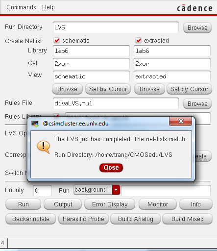
DRC is very important and very time consuming if we don't keep track of. LVS our layout afterward, make sure it matches.
Create a new schematic call sim_gates. Draft the following circuit to test our 3 gates (inverter, nand, and xor).

Let's derive our truth table for all gates.
Inverter
Nand
Xor
Let's simulate our circuit. We'll get the following waveform.

Next
up, create a new schematic call fulladder. We'll draft our fulladder
schematic in. We'll need 2 xor gates and 3 nand gates. There are 3
inputs and 2 outputs.

DRC our circuit, make sure there's no error.
Create a cellview from schematic.

Next up, drafting the layout of our fulladder.
We'll use our premade gates again. This time, we'll need 3 nand gates and 2 xor gates.
I found it easier to have 2 xor gates laying side by side and 3 nand gates laying side by side right next to our xor gates.

Remember when I insist that we leave some room for wiring? This is where it comes in handy.
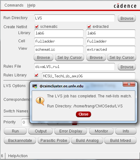
DRC our layout, make sure there's no error. Then LVS our layout make sure it matches!
Create a new schematic call sim_fulladder. We'll draft a circuit that can test our fulladder.

Check and save, set up our simulation for the following output.

Here's our truth table for fulladder. It matches our waveform!
Fulladder
| a | b | cin | s | cout |
| 0 | 0 | 0 | 0 | 0 |
| 0 | 0 | 1 | 1 | 0 |
| 0 | 1 | 0 | 1 | 0 |
| 0 | 1 | 1 | 0 | 1 |
| 1 | 0 | 0 | 1 | 0 |
| 1 | 0 | 1 | 0 | 1 |
| 1 | 1 | 0 | 0 | 1 |
| 1 | 1 | 1 | 1 | 1 |
Let's take it a step further by doing simulation using our extracted view. We should get very similar waveform.

-If we look at our s and cout waveforms,
there are glitches in the outputs of our gates. The glitches happen
during rising and falling edge of our inputs (01,10). This is because
the time it takes for our voltage source to go from 5 to 0 or from 0 to
5 is not ideally 0. The short time delay causes the glitch in our
gates.
Saving My Work!!!
All files and images are backed up in a folder on my desktop,
I'll then send a copy to my email as a backup.
Return to main page here