Lab X - ECE 421L 

Authored by Giang Tran,

10/01/2015


Lab Description

-Design, layout, and simulation of a CMOS inverter.

-Going through Tutorial 3


Pre-lab

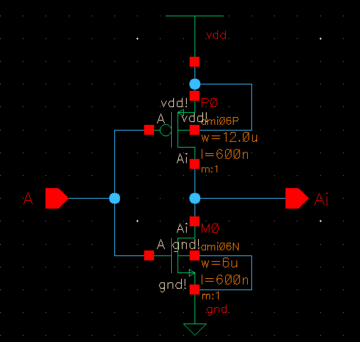
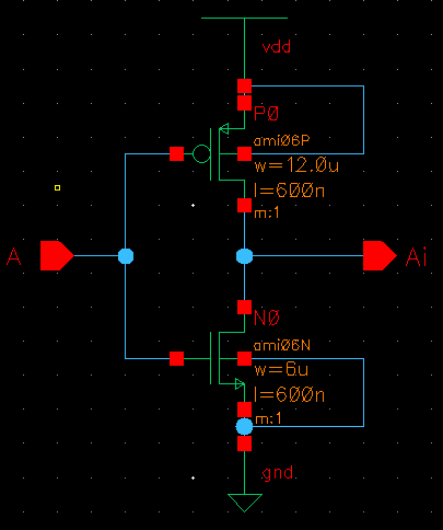
-We'll start off by making a new library called Lab5 then create a new schematic. We'll instantiate our 6 um by 600 nm NMOS and our 12 um by 600 nm PMOS in the previous lab. We'll add vdd to our source terminal in our PMOSand ground our source terminal on NMOS. Name our input terminal A and output terminal Ai like below.

http://cmosedu.com/jbaker/courses/ee421L/f15/students/trang/Lab5/pre1.PNG


Next, we'll create a symbol for our inverter.

http://cmosedu.com/jbaker/courses/ee421L/f15/students/trang/Lab5/pre2.PNG


Create a new layout for our inverter. We'll need:
        1 PMOS
        1 NMOS
        1NTAP
        1 PTAP
        1 M1_POLY
Lay them out like below.

http://cmosedu.com/jbaker/courses/ee421L/f15/students/trang/Lab5/pre3.PNG

Connecting the terminal using metal1 and poly. Notice, our input terminal is connected to the poly of M1_POLY, PMOS and NMOS using a poly layer.

http://cmosedu.com/jbaker/courses/ee421L/f15/students/trang/Lab5/pre4.PNG

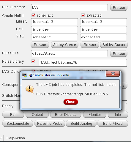
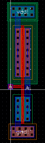
DRC our layout, make sure there's no error. After DRC check, we can proceed and extract our layout view of the inverter.

http://cmosedu.com/jbaker/courses/ee421L/f15/students/trang/Lab5/pre5.PNG

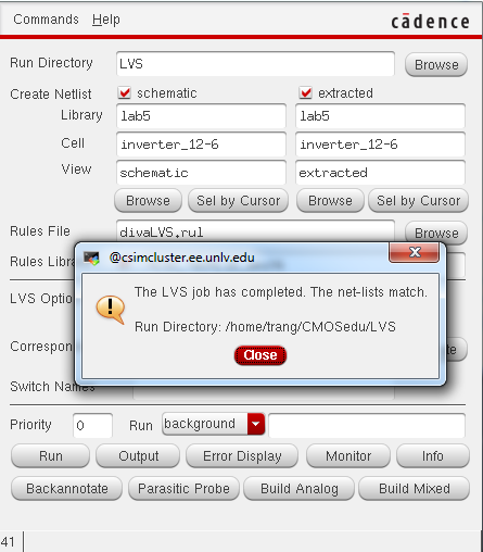
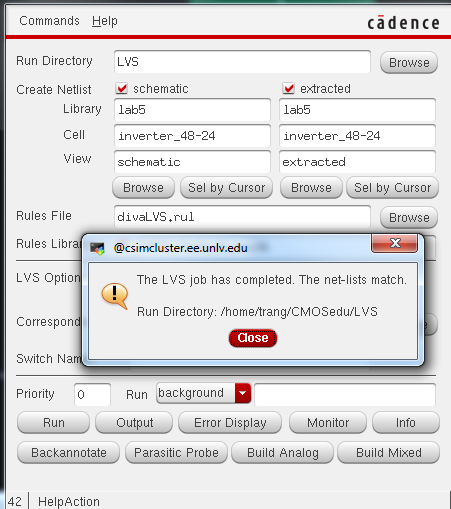
Run LVS, make sure our net-list match.

http://cmosedu.com/jbaker/courses/ee421L/f15/students/trang/Lab5/pre6.PNG.

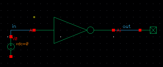
Going back to our library, we'll create a new schematic called sim_inverter.

Add the following circuit to our sim_inverter. 

http://cmosedu.com/jbaker/courses/ee421L/f15/students/trang/Lab5/pre7.PNG

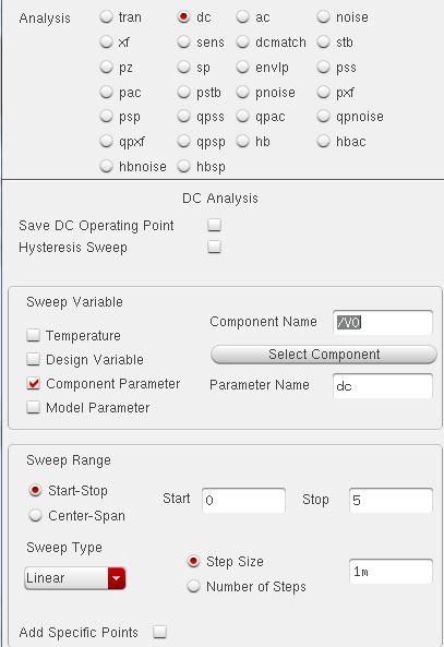
Remember to check and save our circuit. Next, we'll go to ADE then set up our simulation like below.

http://cmosedu.com/jbaker/courses/ee421L/f15/students/trang/Lab5/pre8.PNG

Go to Output >> To be plotted >> On schematic. Select input and out.

Run the simulation, we'll get something similar to this.

http://cmosedu.com/jbaker/courses/ee421L/f15/students/trang/Lab5/pre9.PNG

Notice that our Vout is at 0 V. This is because we did NOT specify a value for VDD.

Going back to our Sim_Inverter, we'll instantiate a vdd with 5 V.

http://cmosedu.com/jbaker/courses/ee421L/f15/students/trang/Lab5/pre10.PNG

Check and save our circuit, then run the simulation again. We'll get something similar to below.

http://cmosedu.com/jbaker/courses/ee421L/f15/students/trang/Lab5/pre11.PNG

Next up, let's simulate our circuit using the extracted layout of our inverter.

Add extracted in front of schematic in Setup -> Environment.

http://cmosedu.com/jbaker/courses/ee421L/f15/students/trang/Lab5/pre12.PNG

Click run, we'll get an identical waveform as above

http://cmosedu.com/jbaker/courses/ee421L/f15/students/trang/Lab5/pre13.PNG

Post-Lab

Again, we're asked to build an inverter with 6 um by 600 nm NMOS and 12 um by 600 nm PMOS. It is easier to copy and paste our inverter from the prelab to a new schematic.

http://cmosedu.com/jbaker/courses/ee421L/f15/students/trang/Lab5/post2.PNG

We'll get an identical circuit 
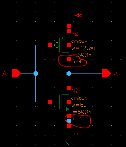
http://cmosedu.com/jbaker/courses/ee421L/f15/students/trang/Lab5/post1.PNG


Notice that our new inverter is 4 times the width of our previous 12u/6u inverter. We'll use multiplier in our NMOS and PMOS when designing the inverter, set M = 4.

http://cmosedu.com/jbaker/courses/ee421L/f15/students/trang/Lab5/post3.PNG

Create cellview for both of our inverters.

http://cmosedu.com/jbaker/courses/ee421L/f15/students/trang/Lab5/post4_1.PNG
http://cmosedu.com/jbaker/courses/ee421L/f15/students/trang/Lab5/post4_2.PNG

Next, we'll create layout view for our inverters. Using NMOS, PMOS,  NTAP, PTAP and M1_POLY, lay them out accordingly.

http://cmosedu.com/jbaker/courses/ee421L/f15/students/trang/Lab5/post5.PNG             http://cmosedu.com/jbaker/courses/ee421L/f15/students/trang/Lab5/post6.PNG
     12u/6u                                                  48u/24u

DRC our layout make sure there's no error. We'll proceed to extracting our layouts

http://cmosedu.com/jbaker/courses/ee421L/f15/students/trang/Lab5/post7_1.PNG   http://cmosedu.com/jbaker/courses/ee421L/f15/students/trang/Lab5/post7.PNG

          12u/6u                                            48u/24u

Next up, we'll LVS our extracted view making sure all pins match!

http://cmosedu.com/jbaker/courses/ee421L/f15/students/trang/Lab5/post8_1.PNG

http://cmosedu.com/jbaker/courses/ee421L/f15/students/trang/Lab5/post8_2.PNG

Simulations

12u/6u inverter simulation without UltraSim

http://cmosedu.com/jbaker/courses/ee421L/f15/students/trang/Lab5/post10_100f.PNG     http://cmosedu.com/jbaker/courses/ee421L/f15/students/trang/Lab5/post10_100p.PNG

                      100f F                                                           100p F

http://cmosedu.com/jbaker/courses/ee421L/f15/students/trang/Lab5/post10_10p.PNG     http://cmosedu.com/jbaker/courses/ee421L/f15/students/trang/Lab5/post10_1p.PNG

                         10p F                                                             1p F


48u/24u inverter without UltraSim

http://cmosedu.com/jbaker/courses/ee421L/f15/students/trang/Lab5/post11_100f.PNG       http://cmosedu.com/jbaker/courses/ee421L/f15/students/trang/Lab5/post11_100p.PNG

                        100f F                                                            100p F

http://cmosedu.com/jbaker/courses/ee421L/f15/students/trang/Lab5/post11_10p.PNG      http://cmosedu.com/jbaker/courses/ee421L/f15/students/trang/Lab5/post11_1p.PNG

                          10p F                                                            1p F

Conclusion: We know that capacitors charge over time, and bigger capacitor requires more time to charge. Therefore, we can see that with a relatively small capacitor, 100f F, the capacitor charges up to 5 V then discharges as the pulse goes back down to 0 V. As we increase the capacitor size from 100f F to 100p F, the capacitor didn't have enough time to fully charged to 5 V then discharged resulting in a sine wave looking response. This can be seen better for 10p F and 1p F capacitors, the response is nearly a straight line. This is because the capacitors did not have sufficient amount of time to either charge or discharge. 

-The inverter was setup so that if A (input) is at 5 V (1). It will turns on our NMOS and output 0 V to Ai. This is because our NMOS is connected to ground, meanwhile, our PMOS stays off (0) because it is inverted. When A is at 0 V (0). Our NMOS is OFF and PMOS is ON; hence, Ai will have an output value of VDD.

Simulation with UltraSim

12u/6u
http://cmosedu.com/jbaker/courses/ee421L/f15/students/trang/Lab5/post12_100f_12.PNG      http://cmosedu.com/jbaker/courses/ee421L/f15/students/trang/Lab5/post12_100p_12.PNG
                         100f F                                                          100p F

http://cmosedu.com/jbaker/courses/ee421L/f15/students/trang/Lab5/post12_10p_12.PNG      http://cmosedu.com/jbaker/courses/ee421L/f15/students/trang/Lab5/post12_1p_12.PNG
                         10p F                                                              1p F

48u/24u
http://cmosedu.com/jbaker/courses/ee421L/f15/students/trang/Lab5/post12_100f_48.PNG      http://cmosedu.com/jbaker/courses/ee421L/f15/students/trang/Lab5/post12_100p_48.PNG
                        100f F                                                          100p F

http://cmosedu.com/jbaker/courses/ee421L/f15/students/trang/Lab5/post12_10p_48.PNG      http://cmosedu.com/jbaker/courses/ee421L/f15/students/trang/Lab5/post12_1p_48.PNG
                          10p F                                                           1p F


Saving My Work!!!

All files and images are backed up in a folder on my desktop,

I'll then send a copy to my email as a backup. 

Return to main page here