Lab 4 - ECE 421L
Authored
by Giang Tran
9/18/2015
trang@unlv.nevada.edu
Lab
description:
-Layout and simulate the operation of NMOS and PMOS using the C5 process.
-Add bonding pads to NMOS and PMOS terminals
Pre-Lab
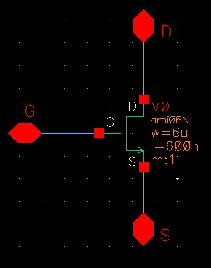
-First,
we'll create a schematic and layout for our NMOS device in a new
library called Tutorial_2. Create an instance called nmos in
NCSU_Analog_Parts window. Our NMOS will have a width of 6u M and a
length of 600n M.
-Next is to add pins according to below.
-Always making sure to run DRC before proceeding to the next step.
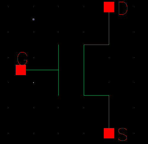
-We'll
create a symbol for the circuit above, click on Create > Cell View
> From Cell View. We'll be drawing a symbol for the circuit so its
neccessary to delete everything except for the 3 pins. Draw a symbol
like below.
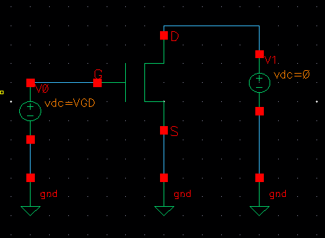
-Next, create a new schematic call sim_NMOS_IV_3
-Add components and wire up the circuit like below
-We will be simulating the circuit using Parametric Analysis

-Our waveform will look similar to this

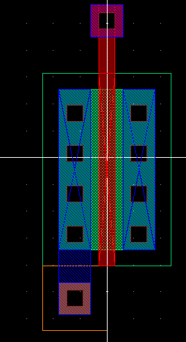
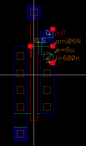
-Close all tabs, we'll make a new layout cell call NMOS_IV_3
-Create
an instance called nmos in the NCSU_TechLib_ami06 library. Again, the
length is 600n M and width is 6u M. Next instantiate a a ptap cell
(metal1 to p+ connection) and a metal1 to poly cell connection line
below.
-Again, DRC your layout making sure it has no error.
-Extract the layout
-Although DRC shows no error but LVS cannot match up the netlist!

-This is because if we look closely at our extracted layout view we'll see pin #4 on the NMOS is missing connection.
-Fix up our layout by adding a pin with global variable gnd! in the ptap cell.
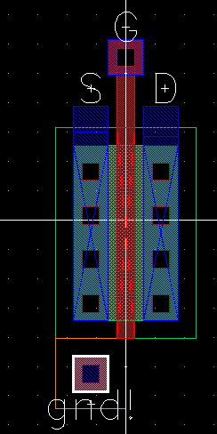
-Look at our new extracted layout view, we'll see the middle pin now is referenced to ground.
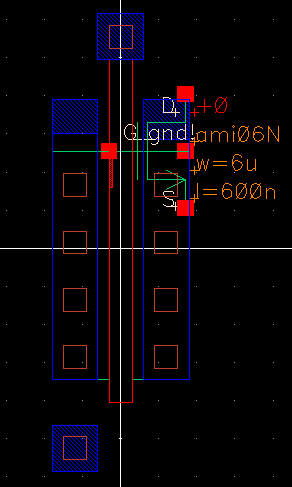
-Although, all pins have connection but LVS wants us to use a 4 legs NMOS instead of 3 legs.

-Go back to the NMOS_IV_3 schematic, we'll place the nmos with nmos4.
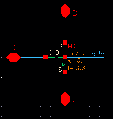
-Run LVS with our new schematic. Netlist match!
-We'll run our simulation again using extracted view. Go to Setup > Environment. Then put extracted in front of schematic.

-Run our Parametric Simulation again

-Next up, we'll create our PMOS using pmos from NCSU_Analog_Parts.
-Create a symbol just like our NMOS.
-Creating
a new cell layout call PMOS_IV. We'll instantiating the following
layout. Our components below are pmos, ptap, and metal1 to poly
connection.
-Check and Save make sure no error is found. We'll make an extracted layout view for the layout.
-Next up, let's create a cell call sim_PMOS_IV. Create the following circuit.
-Run our simulation with schematic view of circuit.

-Next, we want to run simulation again with extracted layout.

Our 2 simulation results look identical to each other!
Post Lab
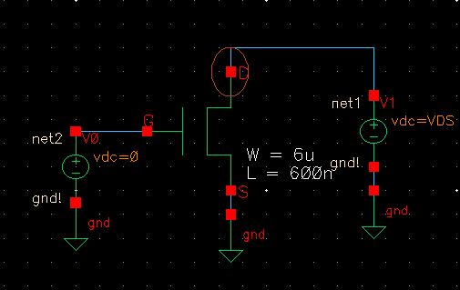
- A schematic for simulating ID
v. VDS of an NMOS device for VGS varying from 0 to 5 V in 1 V steps
while VDS varies from 0 to 5 V in 1 mV steps. Use a 6u/600n
width-to-length ratio.
-We'll
be using parametric analysis for analyzing the circuit. Set up dc
analysis with VDS varies from 0 to 5 V with 1 mV steps. We then define
a new variable for VGS with a value of 0 V. Make sure we're plotting
the current at drain like the picture below.

Doing a parametric analysis with VGS from 0 to 5 V ata linear step of 1 V. We'll get a waveform similar to below.

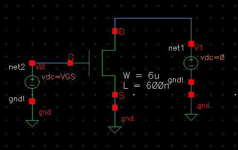
- A
schematic for simulating ID v. VGS of an NMOS device for VDS = 100 mV
where VGS varies from 0 to 2 V in 1 mV steps. Again use a 6u/600n
width-to-length ratio.
-Notice our V0 is at 0 V and V1 = VDS.
-Again,
we're doing dc analysis with V0 varies from 0 to 2 V with a linear step
of 1 mV. Define a new variable name VDS with value of 100 mV and plot
the current at drain. We'll run a parametric analysis on the circuit
and get the following response.

- A
schematic for simulating ID v. VSD (note VSD not VDS) of a PMOS device
for VSG (not VGS) varying from 0 to 5 V in 1 V steps while VSD varies
from0 to 5 V in 1 mV steps. Use a 12u/600n width-to-length ratio.

Set up the analysis like below

We'll the following response:

- A
schematic for simulating ID v. VSG of a PMOS device for VSD = 100 mV
where VSG varies from 0 to 2 V in 1 mV steps. Again, use a 12u/600n
width-to-length ratio.

After setting up the analysis parameters, we'll get the following response:

- Lay
out a 6u/0.6u NMOS device and connect all 4 MOSFET terminals to probe
pads (which can be considerably smaller than bond pads [see MOSIS design rules]and directly adjacent to the MOSFET (so the layout is relative small).
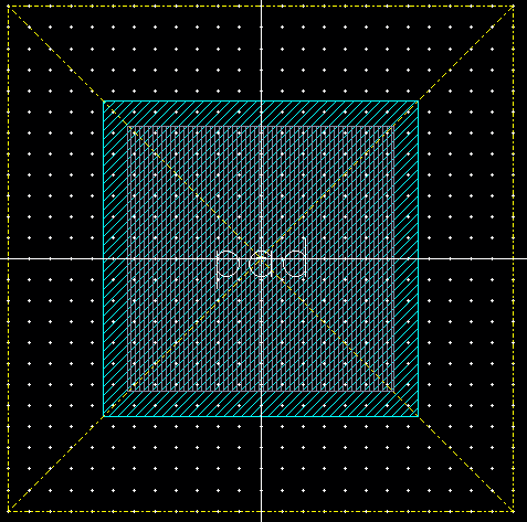
-We can use our bond pad created from previous Tutorial_6, but I went ahead and create a new pad layout to refresh my memory.
After the pad is created, I went ahead and connect the NMOS device terminals to 4 different pads.

We'll
ensure the connections of metal1, metal2, and metal3 are perfect by
having multiple via(s) in 1 connection. We definitely want bigger wires
as safety for electromigration.

Remember to DRC check everytime we made a new metal connection. I found it time consuming by fixing the design rules of spacing.

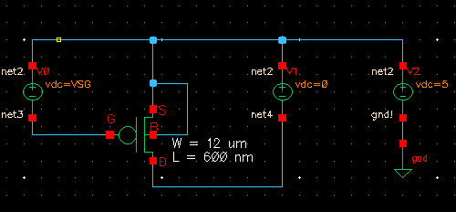
Next up, we'll create a new schematic for the NMOS device with 4 pads connected to its 4 terminals.

Going
back to our layout for LVS check. It is crucial that you use the same
terminal name for both layout and schematic or LVS will not work!

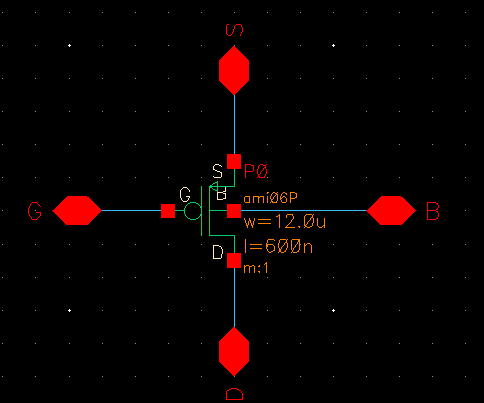
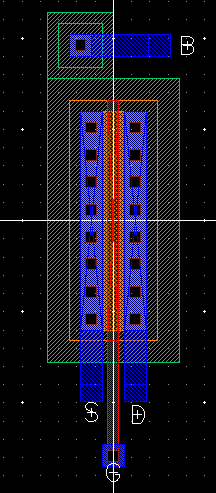
- Lay out a 12u/0.6u PMOS device and connect all 4 MOSFET terminals to probe pads.
Our PMOS device layout connected to 4 pads in each of its terminal can be seen below.

-Always
making sure that you DRC your layout as you wire them up. When you're
finished and DRC shows no error, you can go ahead and extract the
layout.
-After
the layout extraction, we'll create a new schematic for the PMOS device
with 4 bond pads connected to its 4 terminals like below:

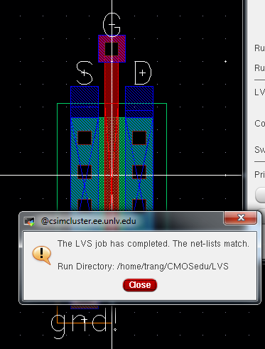
-Going back to our layout window to LVS our files.

-LVS job completed and net-list match!!!!!
Saving My Work!!!
All files and images are backed up in a folder on my desktop,
I'll then send a copy to my email as a backup.
Return to main page here