Lab 3 - ECE 421L
Authored
by Giang Tran
9/12/2015
trang@unlv.nevada.edu
Lab
description:
-Designing 10K resistor using n-well.
-Designing 10-bit DAC using n-well resistors.
Pre-Lab
-The very first step in designing our 10K Ohms resistor is to calculate the length and width of our resistor.
-Using the equation below to calculate for resistance:
-- R = Sheet Resistance * (Length/Width) --
-We
know R = 10K, Sheet Resistance = 800 Ohms/Square. Sheet resistance is
fixed, therefore, we can vary the width and length to get the
resistance we want. I used a width of 4.5 um and length of 56.25 um.
-The
design rules state that our length and width must be divisible by 0.3.
We'll use a higher value for our length in order to meet the
specification, which is 56.4 um.
--Laying the n-well

--Next, press I to open instance then choose ntap cell in NCSU_TechLib_ami06 library.

--Continue by placing ntap, pin names and a layer of res_id over our n-well.

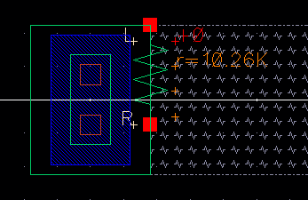
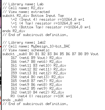
--Now, extract the layout to get extracted view of our resistor. My resistor has a value of 10.26K Ohms.
--Make
a new cell called Mydesign_DACnwell and place 3 n-well resistors in
parallel. We'll connect them accordingly to our r2_div schematic using
metal1.
--We'll
then name the pins according to our R2_div schematic. It is crucial
that we use similar terminal names as in R2_div, or else it will fail
LVS.

--Click on Verify -> DRC then Verify -> Extracted then Verify -> LVS.
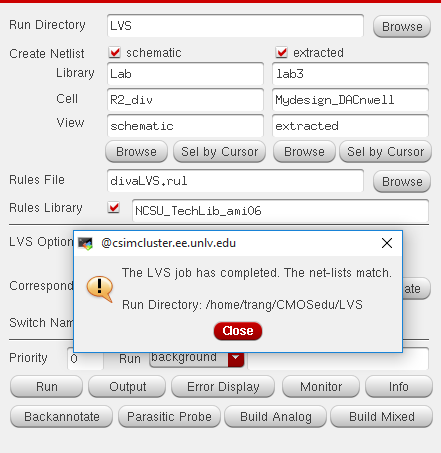
-The
net-lists matched! This is a good sign. We'll proceed to the next step,
which is simulating our ADC_DAC with our extracted file.
-Open
sim2_Ideal_ADC_DAC cell in lab2 library. Run ADE L and load our state
like usual. Next, click on Setup > Environment. We'll add extracted
in front of schematic like below.

-Then run the simulation.
-We
can verify if our simulation is using our extracted view or schematic
view of R2_div. Click on Simulation > Netlist > Display.
It is verified that our simulation is using extracted view. We'll get a waveform similar to below.

--Next, let's implement our DAC using n-well resistors (R2_div) that we created earlier.
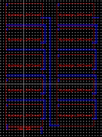
--We'll
be instantiating our layout for R2_div, a total of 10 layouts divided
up into 2 columns (5x5). We will name all the pins accordingly B(0-9),
gnd, and Vout.
--Run LLVS check after DAC and extraction.

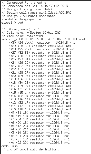
--Verify that our DAC has an extracted view of the circuit.

--Next
up is simulation, we'll be using our old state. Hence, it is necessary
to check if we're simulating through our extracted view or not.
--Finally, let's run our circuit and check out the result.

Download my design directory here!
Saving My Work!!!
All files and images are backed up in a folder on my desktop,
I'll then send a copy to my email as a backup.
Return to main page here