Lab 2 - ECE 421L
Authored
by Giang Tran
8/30/2015
trang@unlv.nevada.edu
Lab
description:
-The purpose of this lab is to use n-well resistors to design 10-bit Digital-to-Analog Converter (DAC).
Pre-Lab
-Our first step is to download a zip file called lab2

-Extract the file using command unzip
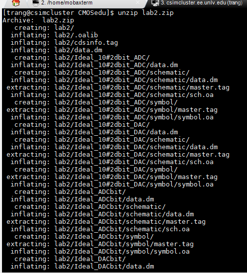
-In order for Cadence to recognize the new library, we need to add DEFINE lab2 $HOME/CMOSedu/lab2 to our cds.lib file.
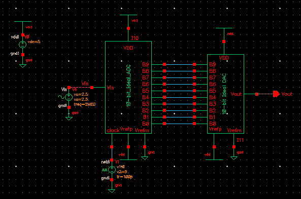
-Next open up sim_Ideal_ADC_DAC schematic in Cadence

The schematic should looks something similar to this!
-Click on ADE L > Session > Load State > Cellview in order to have access to our Analog Design Environment. Click Run
-Our waveform should looks similar to this

Digital-to-Analog Converter
-Is
a function that converts digital binary into an analog signal. A n-bit
DAC has 2^n outputs. In our case, a 10-bit DAC has 2^10 which has 1024
outputs. Our resolution is calculated as 1/2^n which indicates higher
resolution for higher order DAC.
-Our least significant bit can be determined using the following equation Vdd/2^n.
Where n represents our bit and Vdd represents our maximum input
voltage. Hence, our LSB is 5/2^10 = 4.88mV, the lowest voltage value
that will affects our waveform.
Post-Lab

-We're about to implement the above circuit using our own design consists of n-well resistors.

-You can see that I used two 10k resistors in series to implement a 20k resistor like instructed.
-After drafting the schematic, I created a symbol for the schematic for a clean finish.

-After
making our symbol for the n-well resistor, we're about to delay the DAC
and drive a load of 10 pF by grounding pins B[0-8]. Connect B9 to a
pulse source of 0 to 5V.

-Using the equation Td=0.7*R*C, we'll be able to predict the time delay of the circuit. Our Td in this case is 70 ns.
-Our graphical delay time is roughly 75 ns - 5 ns = 70 ns as predicted.

-Next, we'll modify our DAC symbol and schematic in order to use our n-well resistor to implement the DAC as stated before.
-We'll first delete Vrefp, Vrefm, and Vdd on our Ideal DAC symbol since they are not needed in our design.

-Shift-X to go down a layer, we'll replace the circuitry in there with the following

We will name our design as Mydesign_10-bit Ideal DAC. Going back to our ADC to DAC schematic. We'll replace the given DAC with our DAC.

-Driving a 10K load!

-We can see that by add a resistor of 10K Ohms to our circuit. Our output waveform is half of input with no delay.
-Driving a 10 pF Capacitor!


-The capacitor takes longer time period to charge up. Hence, it was necessary to increase the time period in our analysis.
Lastly, RC load!

-In
real circuit the switches are implemented with transistors. If the
resistance of the switches isn't small compare to R, we'll see our
output voltage to decrease. This is because the parasitic resistance of
our transistors would add up with 2R, hence, decrease our output
voltage.
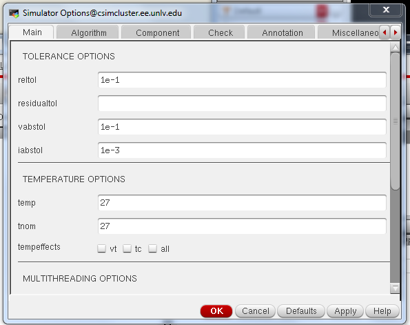
- If you have simulation convergence problems you can force the simulation to converge by going to, in the ADE, Simulation -> Options -> Analog
- Set the values as seen below
- relative tolerance, reltol, of 10% (= 1e-1)
- voltage absolute tolerance, vabstol, of 100 mV (= 1e-1)
- current absolute tolerance, iabstol, of 1 mA (= 1e-3)
- The accuracy of the simulation will, obviously, be degraded
Saving My Work!!!
All files and images are backed up in a folder on my desktop,
I'll then send a copy to my email as a backup.
Return to main page here


