Lab Project - EE 421L
Brandon Thomas (email:thomasb3@unlv.nevada.edu)
November 9, 2015
Objectives:
In this lab we set up all the schematics and did all the simulations
for the things that are going to go on our chips that we are having
fabricated using the C5 Process through MOSIS.
Procedures:
1)
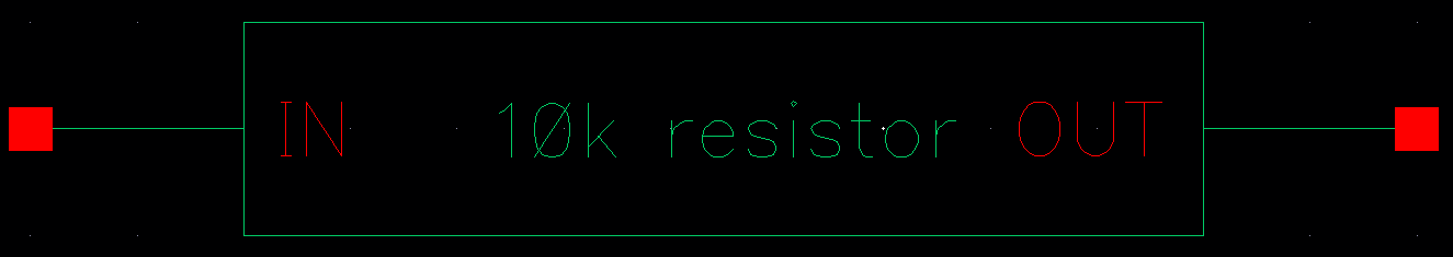
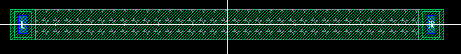
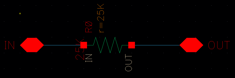
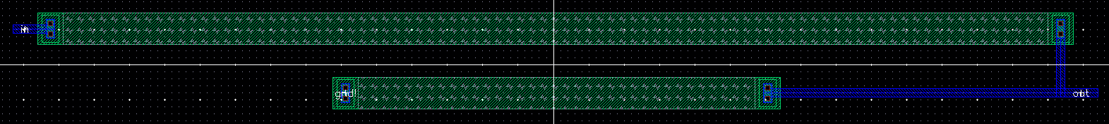
The first step was to set up the 25k and 10k resistors and simulate the
V=IR relationship, and to set up a voltage divider using one of each
and plot the input and output.
10k resistor

25k resistor


Simulation Schematic

Voltage Divider


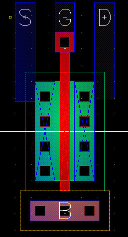
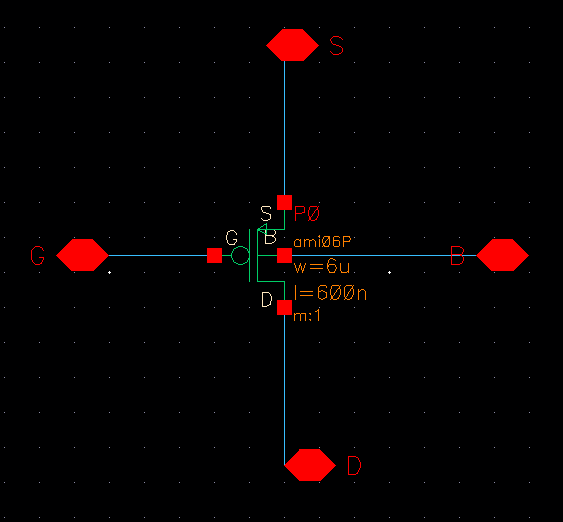
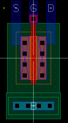
2) The next step was to create a symbol for and simulated the IV curves for both NMOS and PMOS transistors and lay them out.
NMOS


IV simulation (Current versus VDS at different values of VGS)

IV simulation (Current versus VGS)
http://cmosedu.com/jbaker/courses/ee421L/f15/students/thomasb3/Lab_Project/Lab_Project.html
PMOS

IV simulation (Current versus VSD at different values of VSG)

IV simulation (Current versus VSG)

3) The next thing we need to set up and simulate was an inverter with an NMOS of size 6u/0.6u and a PMOS of size 12u/0.6u.

Inverter Simulation

4)
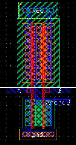
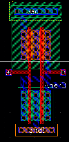
The next thing we need to include on our chips is a circuit
demonstrating the operation of our designed NAND and NOR gates. The
following pictures show their design as well as their simulations.
NAND
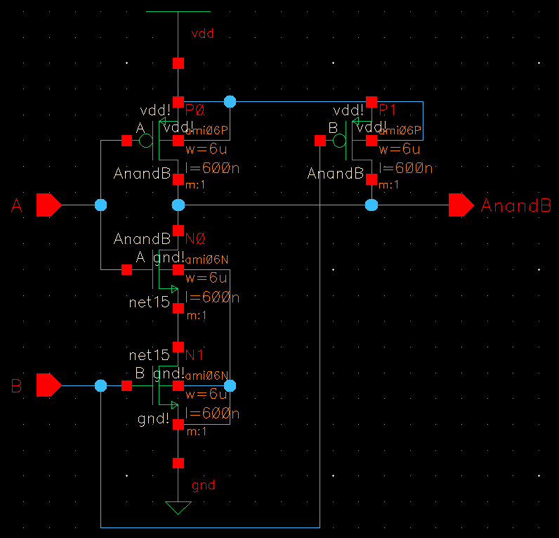
NOR

NAND and NOR simulation schematic


5)
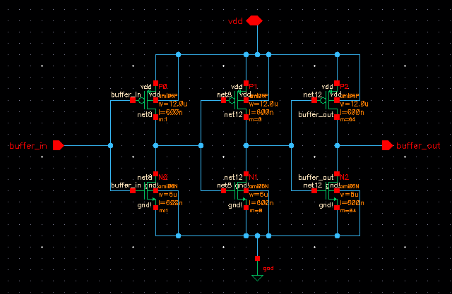
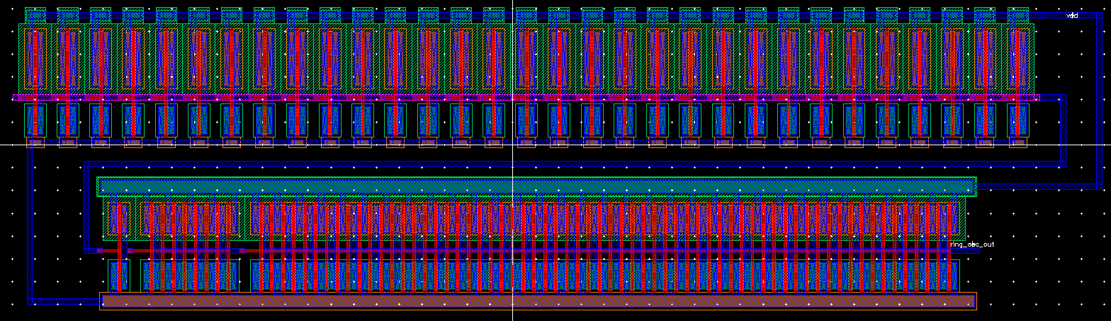
The next thing to be included is the 31-stage ring oscillator, however,
for the oscillator to be useful, there needs to be a buffer at the end
stage of the oscillator.
Oscillator Schematic


Buffer
Ring Oscillator with Buffer Layout
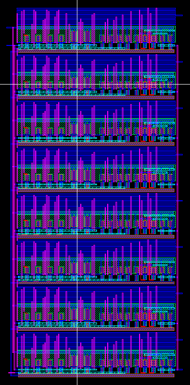
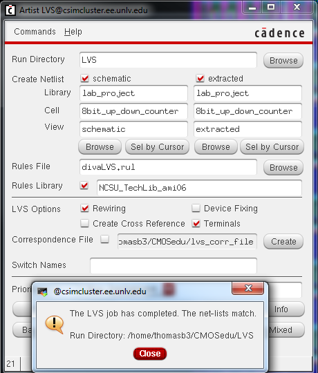
6)
Finally the largest circuit is the 8-bit up/down counter with a clear
input to reset the counter. In order to construct the 8 bit
counter, one of the fundamental building blocks to be used is the
D-Flip-Flop. The D-Flip-Flop will be used to create the one bit
counter which will then be used in the 8-bit counter.
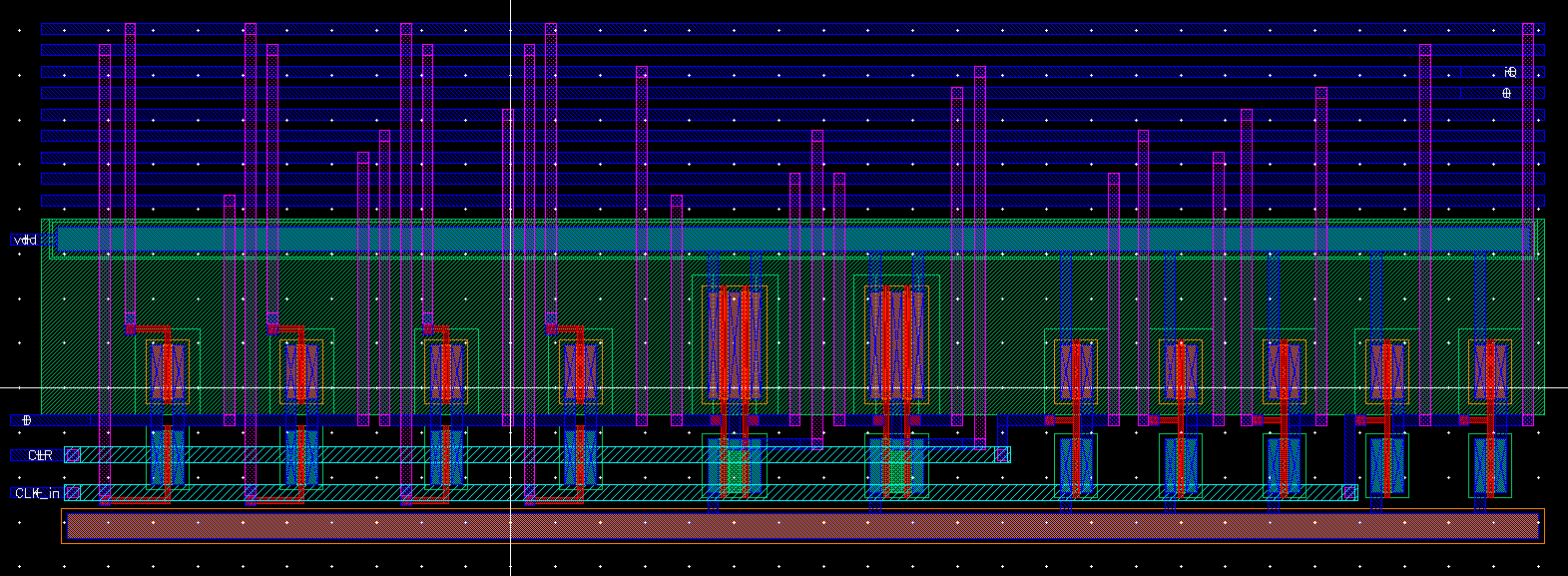
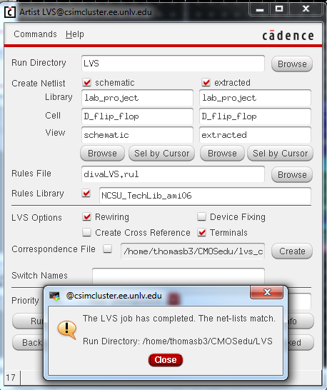
D-Flip-Flop


DFF Layout
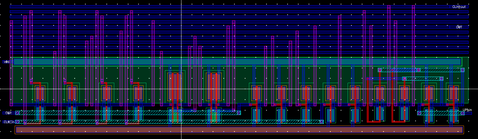
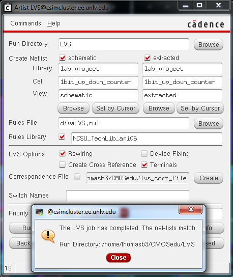
1-bit Up/Down Counter

8-bit Up/Down Counter


Simulation Counting Up

Simulation Counting Down
