Procedures:
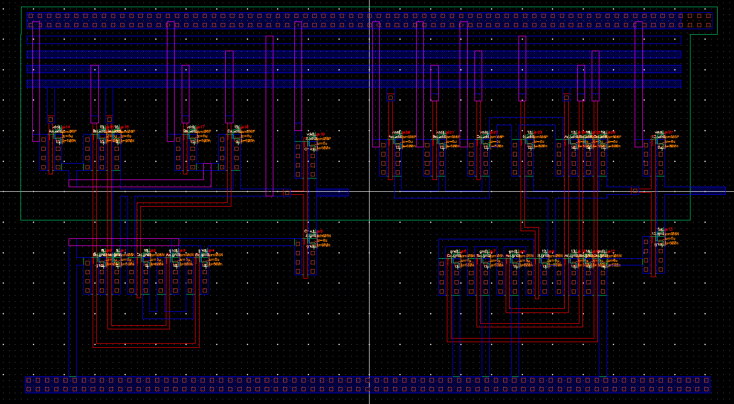
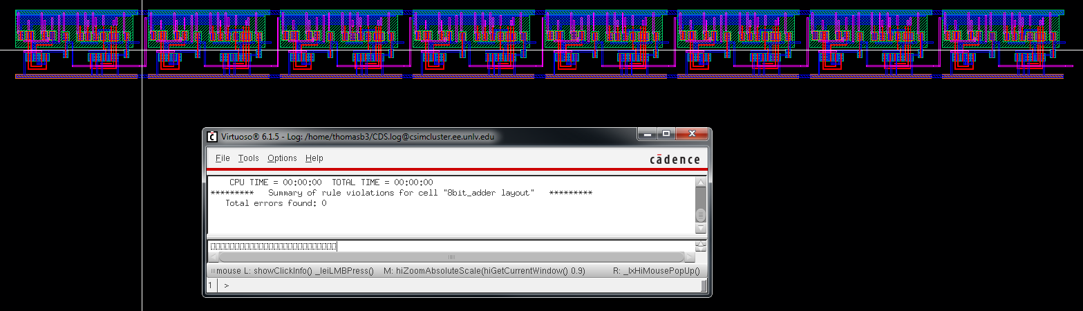
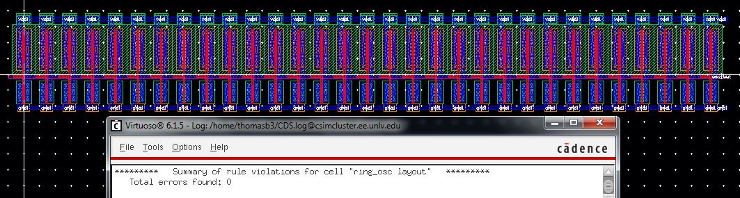
1) The first part of the lab required setting up the schematic and laying out a ring oscillator. The layout of the ring oscillator is seen below along with its DRC test.
Lab 7 - EE 421L
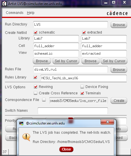
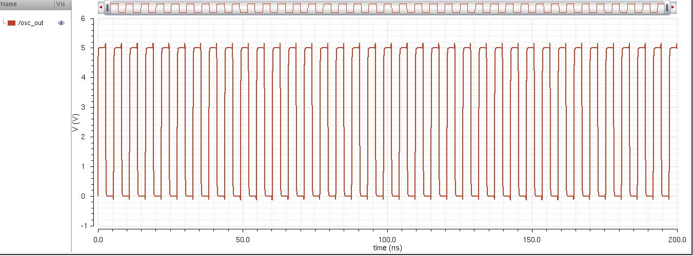
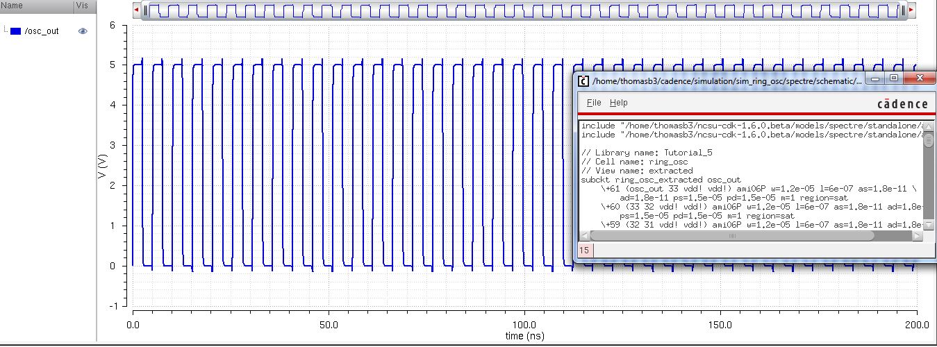
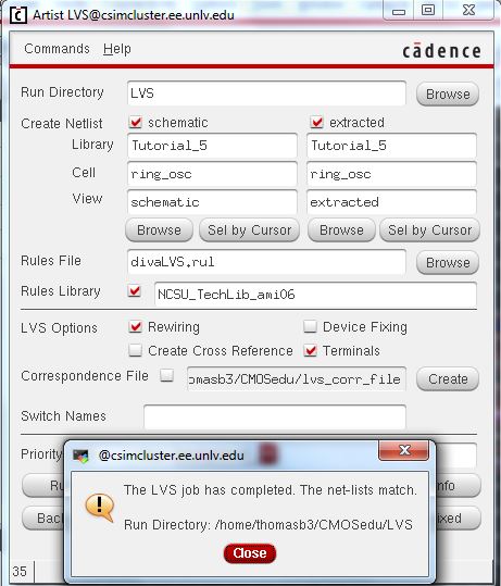
2) We then had to plot the output of the ring oscillatorfrom the schematic and then again from the extracted view followed by LVSing the ring oscillator.
Schematic:
Extracted:
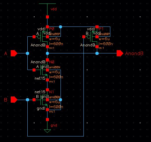
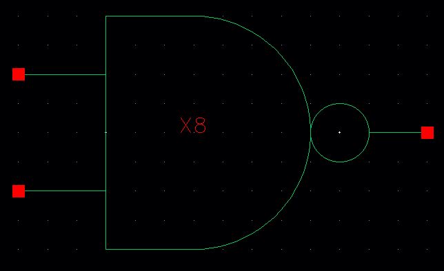
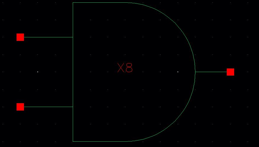
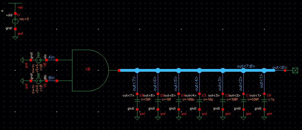
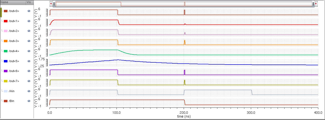
3) After completing the ring oscillator we had to draw up the schematic for the following things: first the schematic for inverting a 4-bitword and test simulations, then the schematics for 8-bit input/output array of: NAND, NOR, AND, OR, and an inverter, as well as the corresponding test simulations for each (I only tested the AND gate and the NOR gate to save time and prevent the lab report).
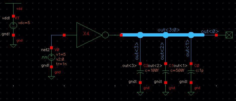
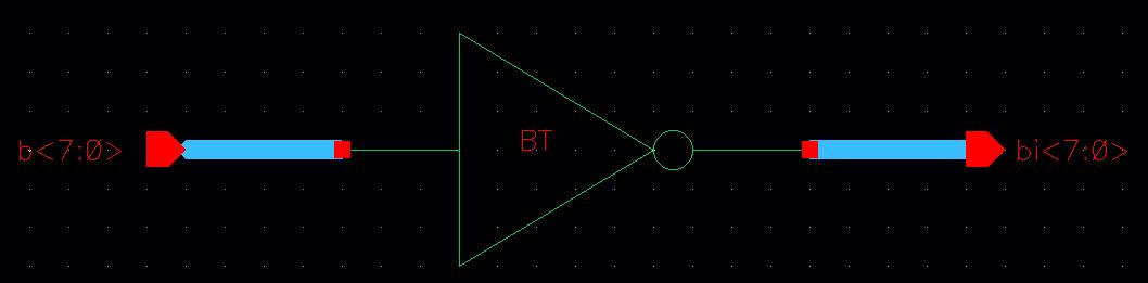
Inverting 4-bit word:
Inverter schematic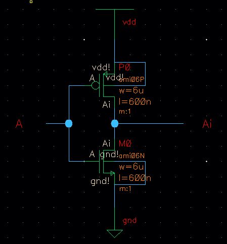
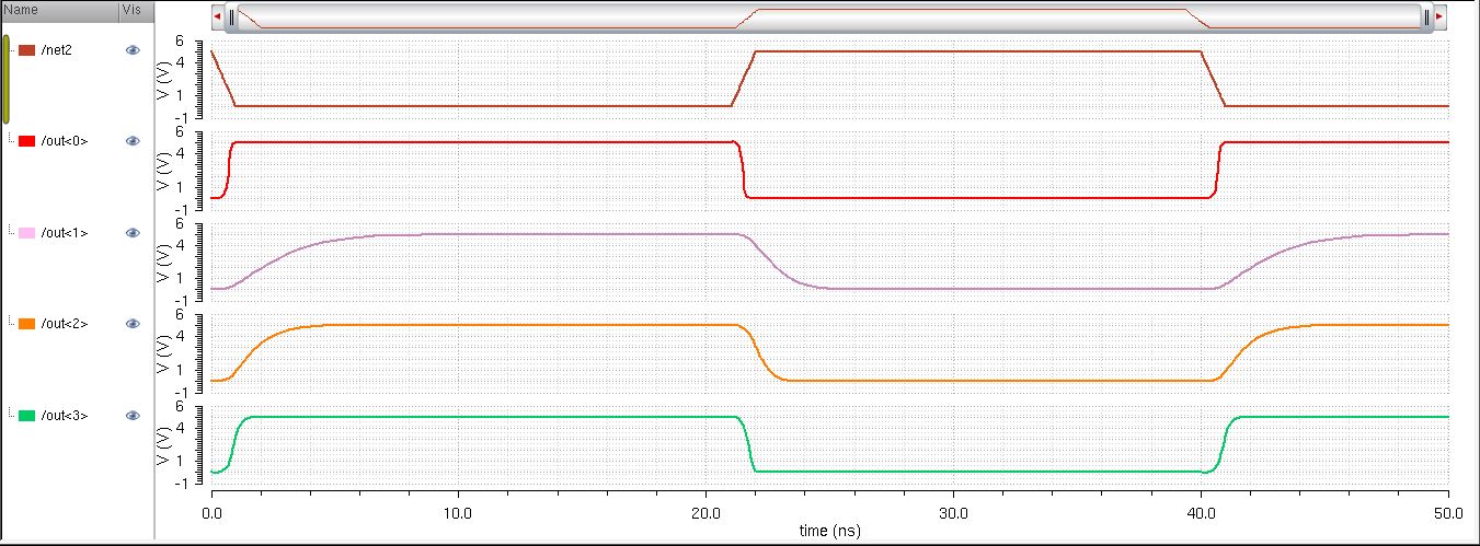
8-bit inverter:
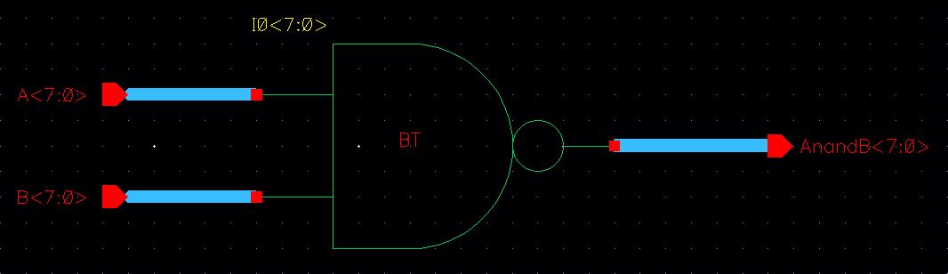
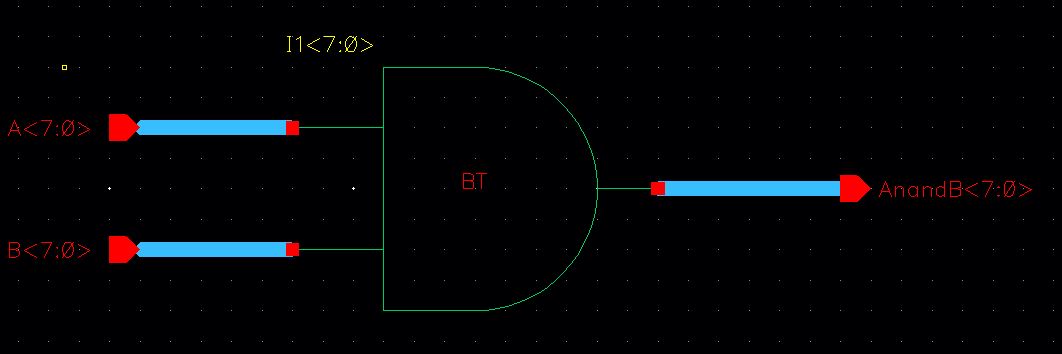
8-bit NAND gate:
NAND gate schematic
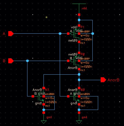
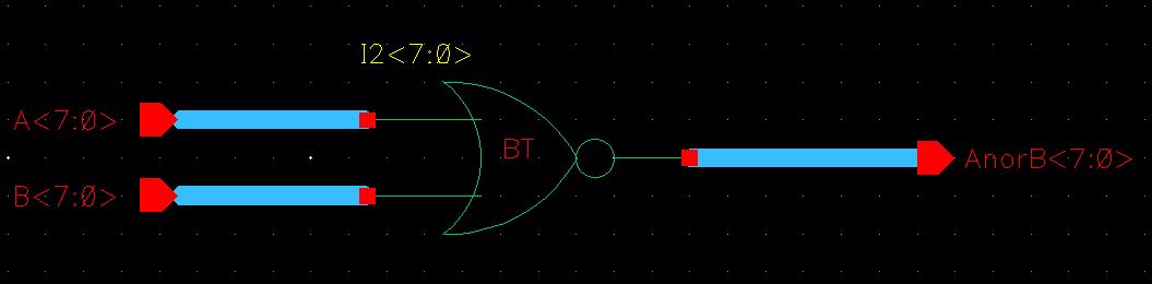
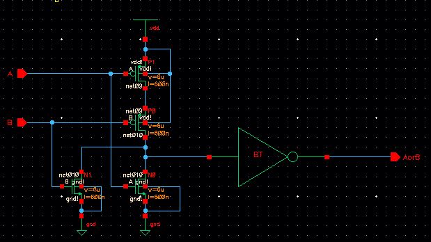
8-bit NOR gate:
schematic
NOR gate sim schematic:
http://cmosedu.com/jbaker/courses/ee421L/f15/students/thomasb3/Lab_Project/Lab_Project.html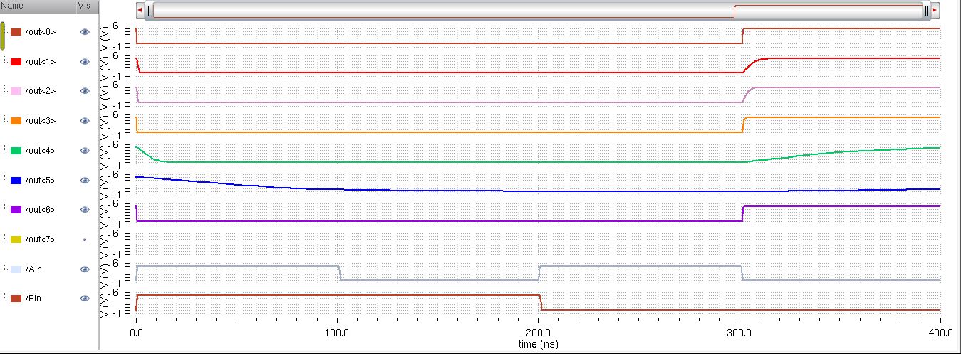
8-bit AND gate:
Schematic
http://cmosedu.com/jbaker/courses/ee421L/f15/students/thomasb3/Lab_Project/Lab_Project.html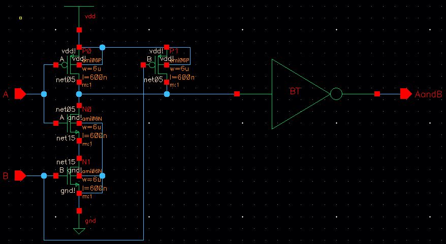
8-bit AND gate sim schematic:
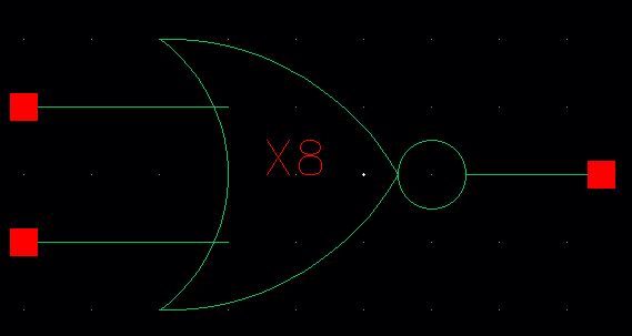
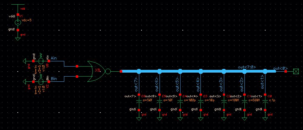
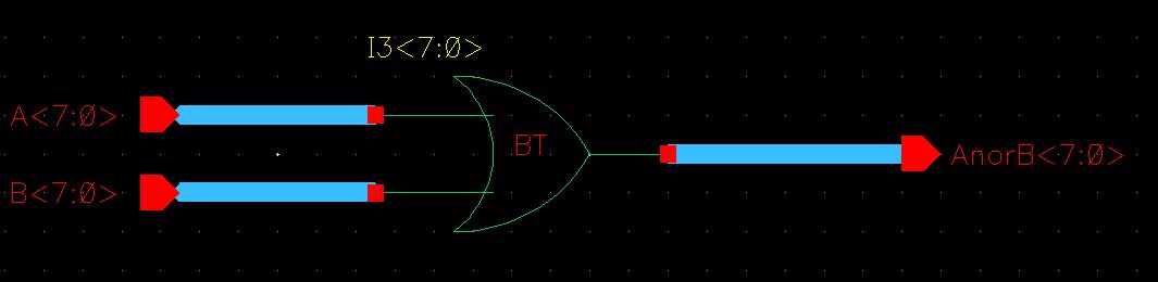
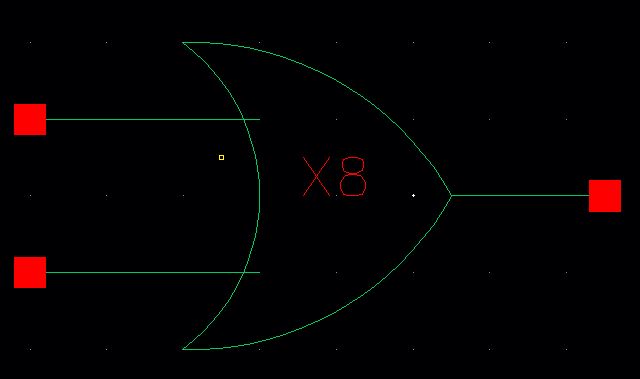
8-bit OR:
Schematic:
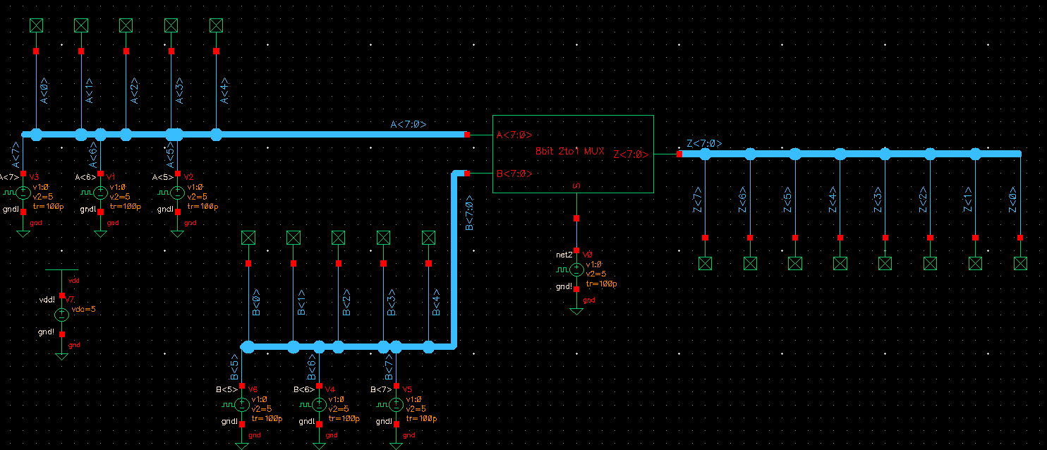
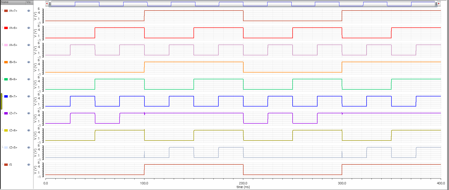
4) The next thing we had to do was create a schematic for a 2to1 DEMUX/MUX and simulate its operation.
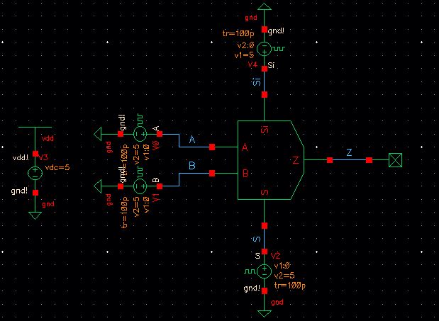
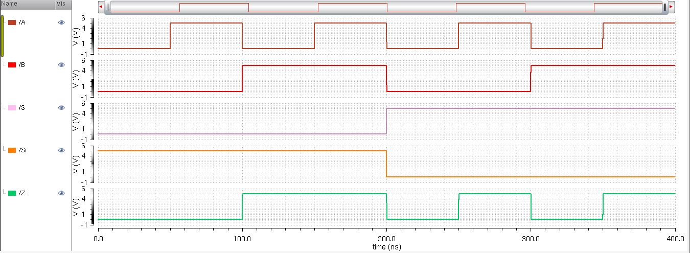
The way the MUX operates is by using the selecter inputs (S and Si) to control transmission gates. When S is a logic high (meaning Si is a logic low) it turns the second transmission gate on allowing the B signal to pass through and vice versa for the input A.
5) The next part of the lab was taking the 2-to-1 MUX we just created and using it to create an 8bit wide word 2-to-1 MUX. The first step of this was to set up the schematic for it and create a symbol of the schematic for use in a simulation schematic.