Lab 6 - EE 421L 

Brandon Thomas (email:thomasb3@unlv.nevada.edu)

October 19, 2015


Objectives: In this lab we had to make the schematics for the NAND gate and the XOR gate using transistors as well as create their respective layouts.  After creating the gates, we then had to use these gates in an implementation of a full adder.  Once the schematic was created we also had to setup the layout for the full adder as well using the previously designed layouts for the NAND and XOR gates.  

Procedures: 

1) We had to start this lab off by completing Tutorial 4 in which we created the NAND gate.  The first thing we had to do was set up the schematic for the gate using NMOS and PMOS transistors.  A simulation was then done to test the NAND gate.  The following images were the results:

file:///C:/Users/Sandy/Desktop/Brandon%20College/EE421/Lab/Lab6/NAND_schematic.JPG

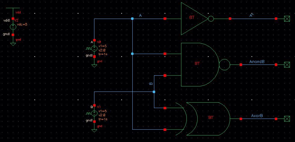
This was the setup used to test the NAND gate; only one of the inputs was changed while the other was held constant.

file:///C:/Users/Sandy/Desktop/Brandon%20College/EE421/Lab/Lab6/NAND_B_input_pulse_schematic.JPG

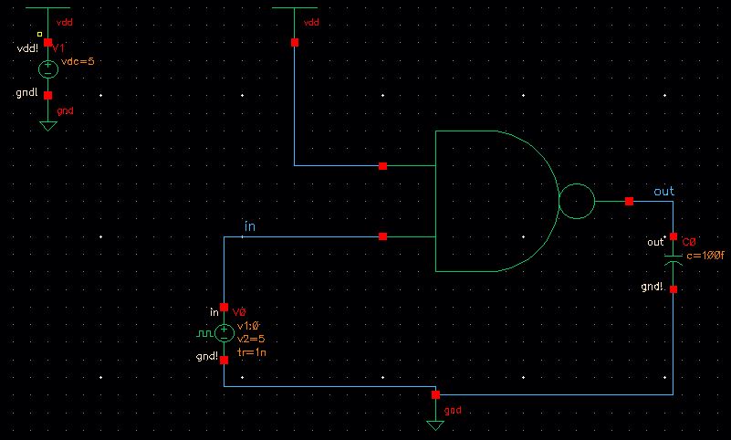
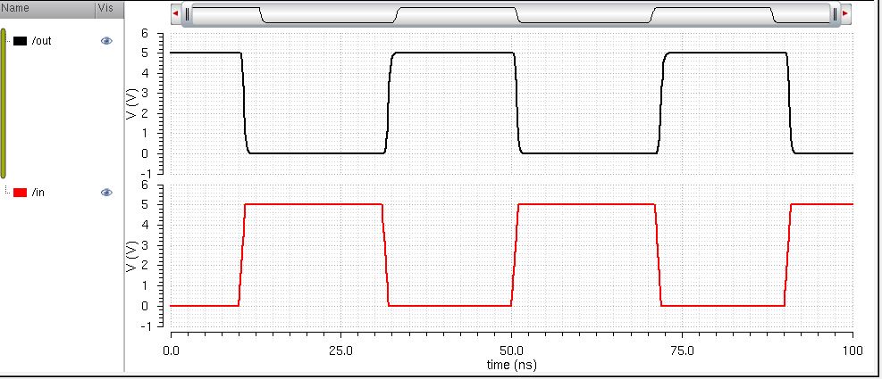
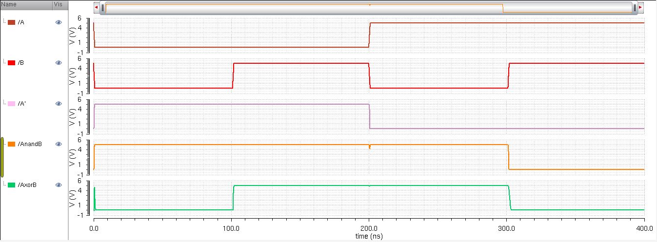
The following plot resulted when the input and output pins were probed.

file:///C:/Users/Sandy/Desktop/Brandon%20College/EE421/Lab/Lab6/NAND_B_input_pulse_sim.JPG

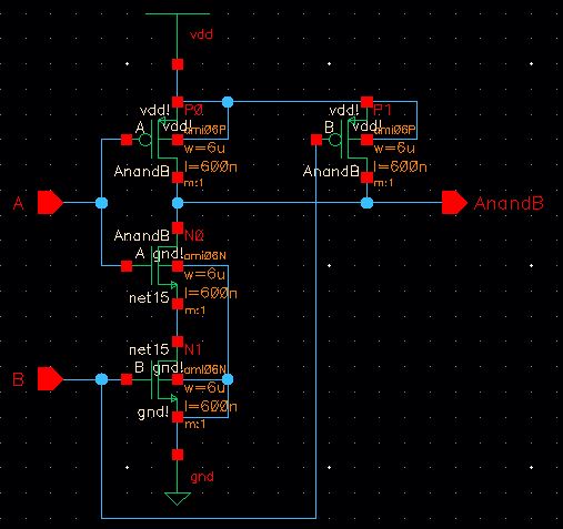
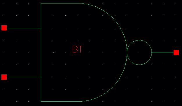
We also had to create a symbol for the NAND gate that we could use when designing the full adder.

file:///C:/Users/Sandy/Desktop/Brandon%20College/EE421/Lab/Lab6/NAND_symbol.JPG

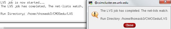
After setting the schematic up, the next step was to layout the gate, DRC the layout, then extract it and LVS check it.


                        Layout                                                Extracted

file:///C:/Users/Sandy/Desktop/Brandon%20College/EE421/Lab/Lab6/NAND_layout.JPG                file:///C:/Users/Sandy/Desktop/Brandon%20College/EE421/Lab/Lab6/NAND_extracted.JPG

file:///C:/Users/Sandy/Desktop/Brandon%20College/EE421/Lab/Lab6/NAND_layout_first_drc.JPG

file:///C:/Users/Sandy/Desktop/Brandon%20College/EE421/Lab/Lab6/NAND_extracted_LVS.JPG

2) After completing the tutorial, we then had to design an XOR gate.  The XOR gate had the same requirements as the NAND gate, the first of which was to set up the schematic and create a symbol for it.

file:///C:/Users/Sandy/Desktop/Brandon%20College/EE421/Lab/Lab6/XOR_schematic.JPG

file:///C:/Users/Sandy/Desktop/Brandon%20College/EE421/Lab/Lab6/XOR_symbol.JPG

Once the symbol was made, we had to use this symbol as well as the symbols we created for the NAND gate and the inverter from lab 5 in a single test circuit.

file:///C:/Users/Sandy/Desktop/Brandon%20College/EE421/Lab/Lab6/gate_sim_schematic.JPG

This schematic resulted in the following plots.

file:///C:/Users/Sandy/Desktop/Brandon%20College/EE421/Lab/Lab6/gate_sim.JPG


Then next step was then to layout the XOR gate, make sure it passes DRC, extract the layout, and make sure the LVS passes, just as in the case of the NAND gate.  The layout ended up looking pretty messy:

                                        Layout                                                                                            Extracted
file:///C:/Users/Sandy/Desktop/Brandon%20College/EE421/Lab/Lab6/XOR_layout.JPGfile:///C:/Users/Sandy/Desktop/Brandon%20College/EE421/Lab/Lab6/XOR_extracted.JPG
   
file:///C:/Users/Sandy/Desktop/Brandon%20College/EE421/Lab/Lab6/XOR_layout_drc.JPG
file:///C:/Users/Sandy/Desktop/Brandon%20College/EE421/Lab/Lab6/XOR_extracted_LVS.JPG

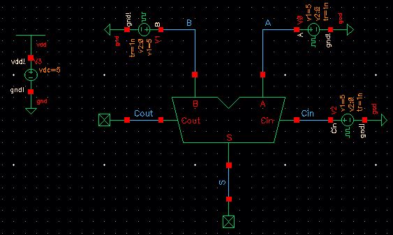
3) Once we established that our gates were working correctly, we then had to use them to create the full adder.  The first task for creating the full adder was laying out the schematic.

file:///C:/Users/Sandy/Desktop/Brandon%20College/EE421/Lab/Lab6/full_adder_schematic.JPG

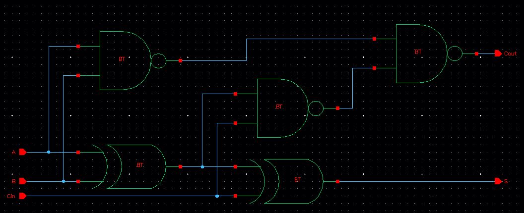
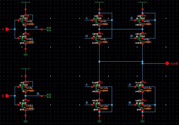
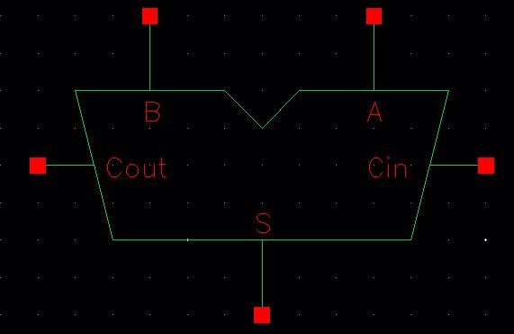
We created a symbol for the full adder so that it could also be tested using the following schematic.

file:///C:/Users/Sandy/Desktop/Brandon%20College/EE421/Lab/Lab6/full_adder_symbol.JPG

file:///C:/Users/Sandy/Desktop/Brandon%20College/EE421/Lab/Lab6/full_adder_sim_schematic.JPG

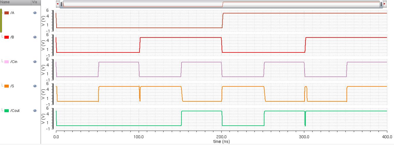
The full adder test schematic produced the following plot

file:///C:/Users/Sandy/Desktop/Brandon%20College/EE421/Lab/Lab6/full_adder_sim.JPG

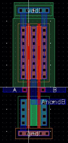
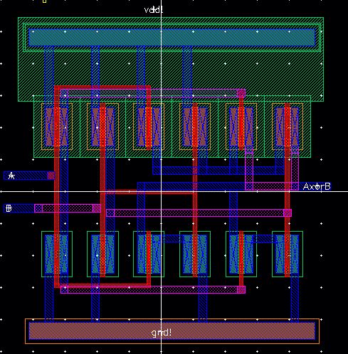
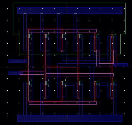
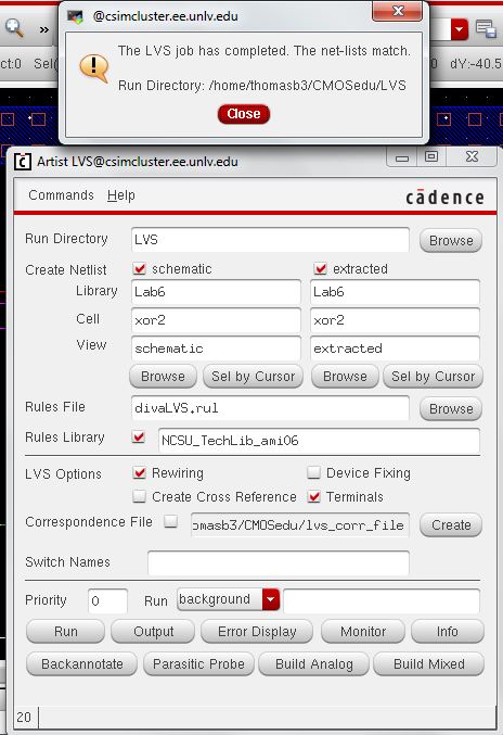
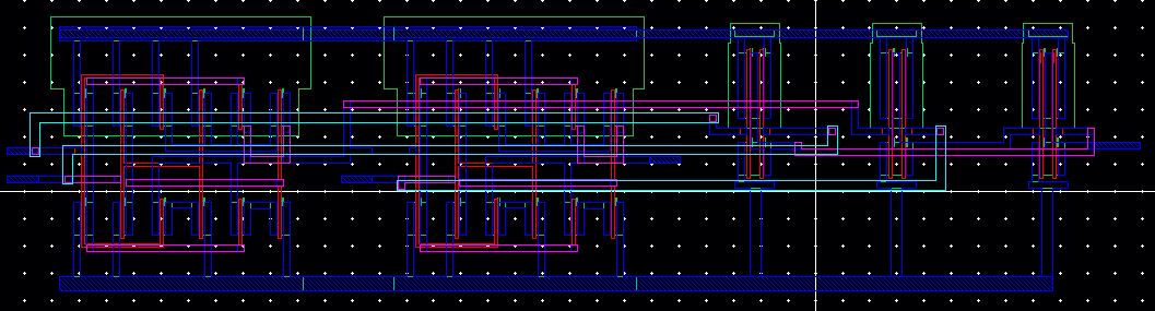
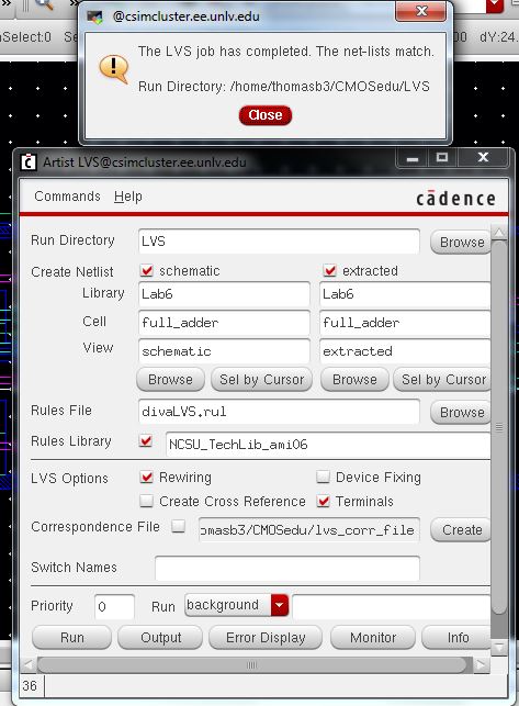
4) After completing the stuff regarding the schematic of the full adder, we had to design the layout of the full adder, make sure it DRCs, then extract the layout, make srue it passes LVS.
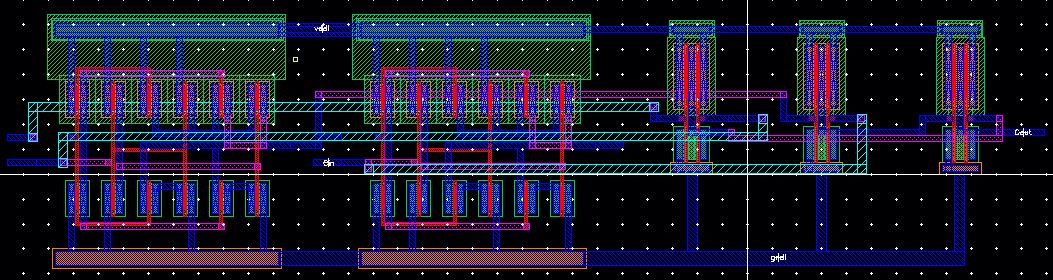
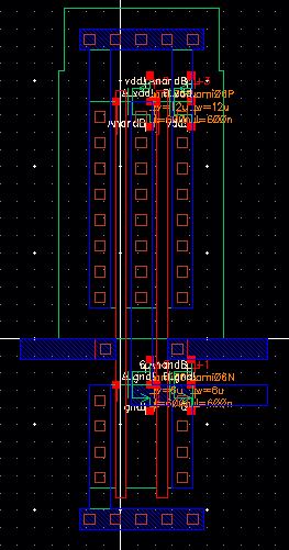

Layout

file:///C:/Users/Sandy/Desktop/Brandon%20College/EE421/Lab/Lab6/full_adder_layout.JPG

Extracted

file:///C:/Users/Sandy/Desktop/Brandon%20College/EE421/Lab/Lab6/full_adder_extracted.JPG

file:///C:/Users/Sandy/Desktop/Brandon%20College/EE421/Lab/Lab6/full_adder_drc.JPG

file:///C:/Users/Sandy/Desktop/Brandon%20College/EE421/Lab/Lab6/full_adder_extracted_lvs.JPG

Conclusions:

The main that I learned from this lab and concluded from everything that the lab involved is that laying out something as simple as a full adder is way more complicated than I ever imagined.  The amount of wiring required was crazy, and became somewhat difficult to follow.  The hardest part for me was laying out the XOR gate.  Making sure all the terminals of all the transistors were laid out properly was very tedious.  However, it started to not look as daunting as it was originally when i finally got to laying out the full adder.  That was nowhere near as challenging but a few errors did arise when performing the LVS test.  The errors turned out to be due to things not being connected, which luckily didn't take too long to figure out.  It just showed me how careful you have to be when laying out these devices. 

Return to the lab page here