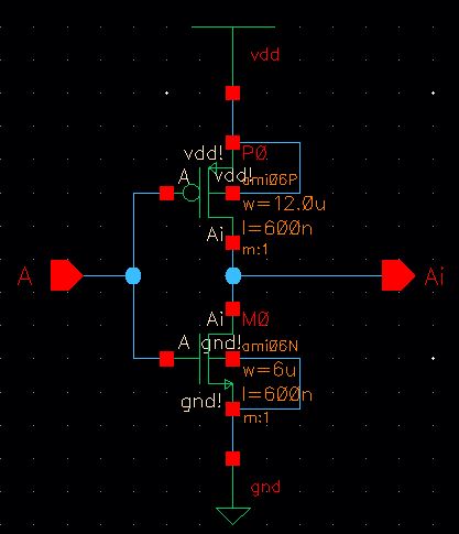
Lab 5 - EE 421L
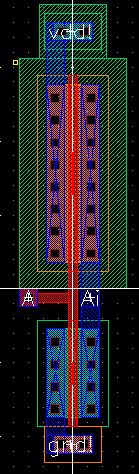
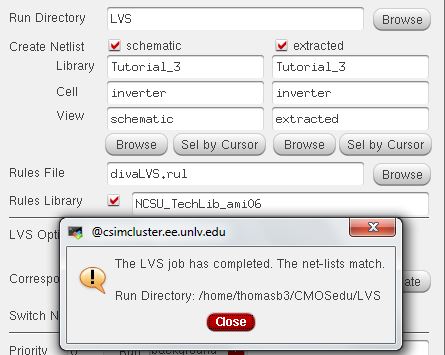
2) After creating the symbol for the inverter, we created the layout and the extracted layout of the schematic, which had to pass DRC and LVS tests.
layout: extracted:
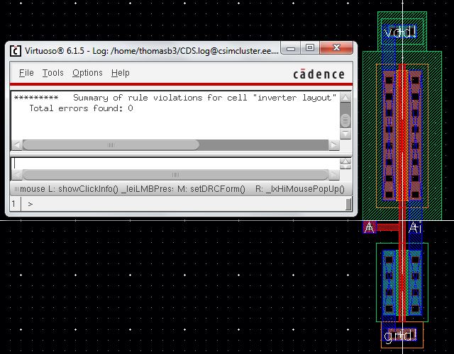
LVS test pass:
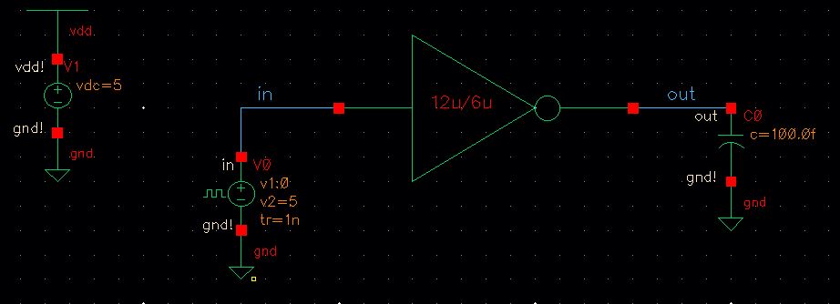
The general simulation schematic looked like the picture below. The only difference between each was the load (the capacitor's
value was changed every time, except for the general simulation in which there was no load).
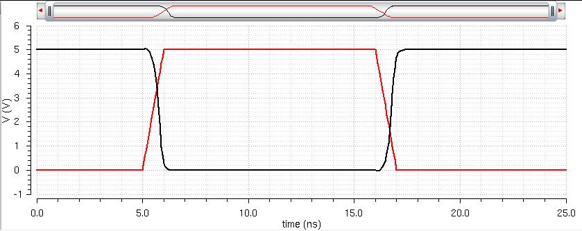
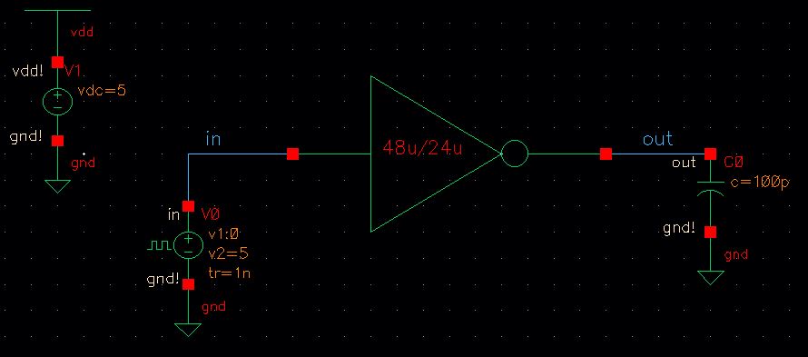
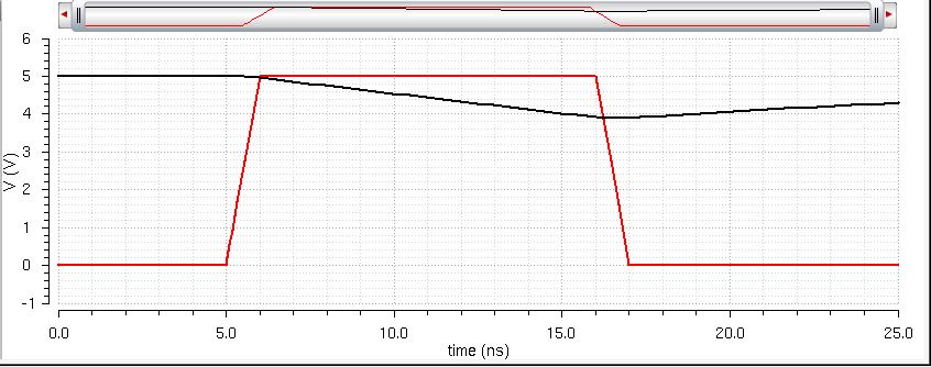
100fF capacitor load
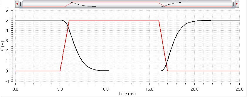
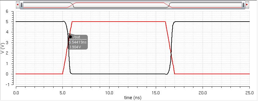
1pF capacitor load:
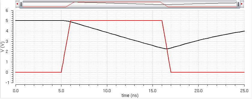
10pF capacitor load:
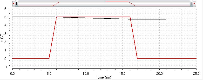
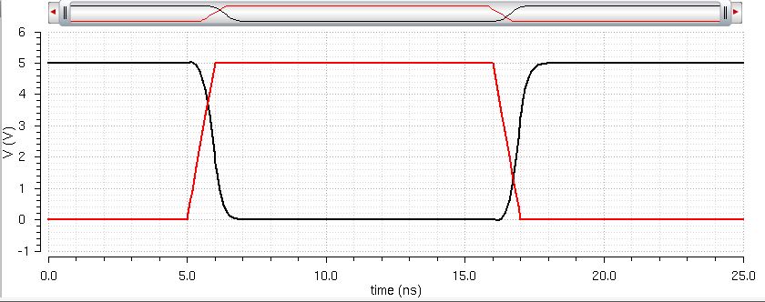
100pF capacitor load:
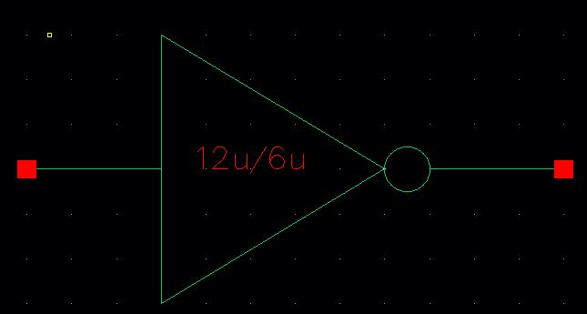
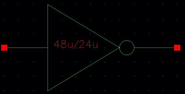
4) After making the regular inverter schematic and symbol and doing the simulations for each output, we made the inverter that implemented the 4x multiplier. The onlydifference between the 4x multiplier schematic and the regular inverter schematic is the multiplier value which could be changed in the properties of each MOSFET. From the schematic, the symbol for the 4x-multiplier symbol was created, and was labeled according to its size.
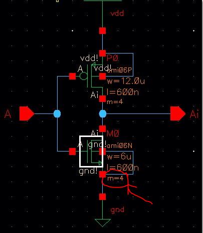
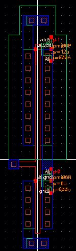
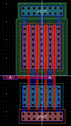
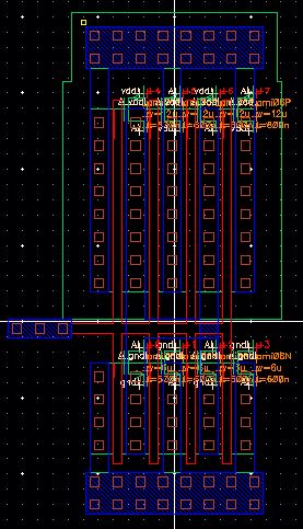
5) Again, the layout and extracted views of the multiplier inverter were created after finishing the schematic and symbol.
layout: extracted:
6) The same simulations were performed using the 4x-multiplier inverter.
The general simulation schematic looked like the picture below. The only difference between each was the load (the capacitor's
value was changed every time).
100fF capacitor load:
1pF capacitor load:
10pF capacitor load:
100pF capacitor load:
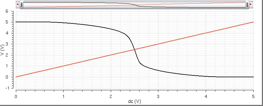
Conclusions: The main conclusion to be drawn from this lab is how the the different multiplier, or in other words the inclusion of more paths for charge to travel, helps the inverter drive a larger load more easily. Of course there is a point at which the larger inverter cannot supply enough current, quickly enough to invert the signal to the output load. This is exactly what happened with the 100 pF load. However, the larger inverter was able to handle the 10pF load a lot better than the smaller inverter. It still was not perfect of course but the inversion of the signal did take place as opposed to the smaller inverter, where the output voltage dropped to 2.5 before starting to return to the originial 5V voltage. When performing the simulations using UltraSim, none of the actual plots were changed. The only difference was that the plot appeared faster than when normally using spectre.