Lab 4 - ECE 421L
Brandon Thomas (email:thomasb3@unlv.nevada.edu)
September 28, 2015
In
this lab we were supposed to create the schematics and layouts for NMOS
and PMOS transistors, as well as simulate and plot the the IV curves of
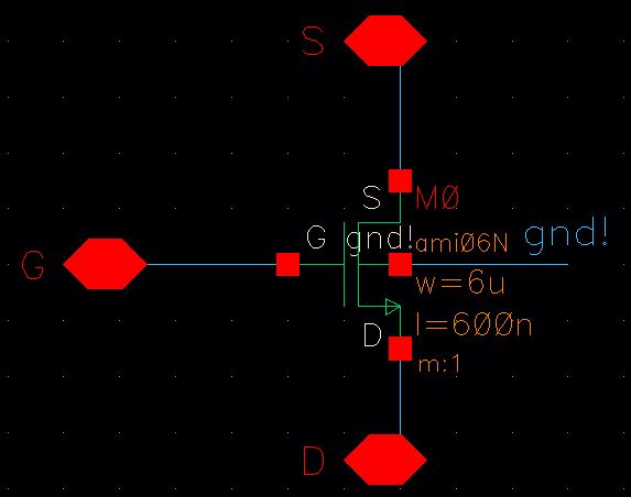
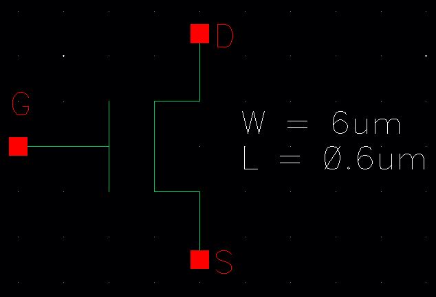
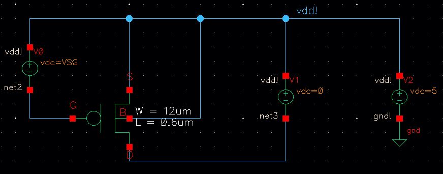
each. We started off by making the NMOS and attaching pins to it
followed by creating the symbol for it so that we could use it for
plotting the IV curves.
We then used this symbol in the creation of a schematic, which was used to plot the IV curves of the NMOS.
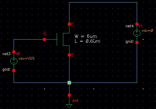
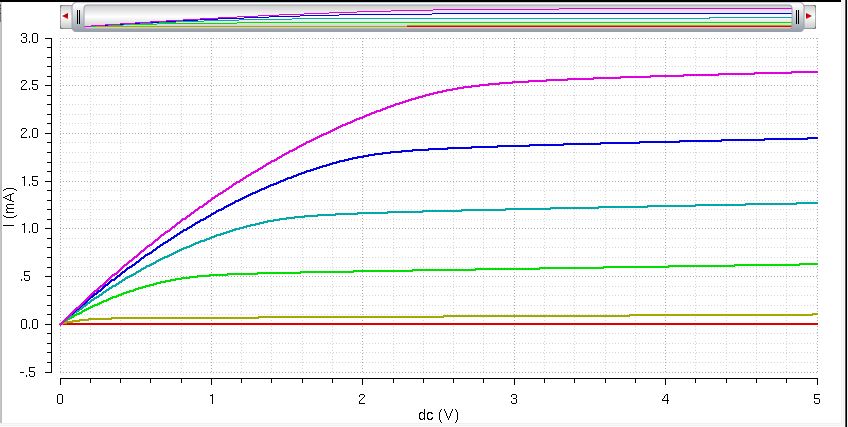
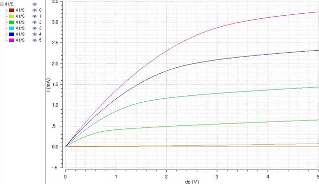
This
plot was based off the fact that VGS was varying from 1 to 5V in 1V
intervals, while VDS was being swept from 0 to 5V in 1mV intevals.
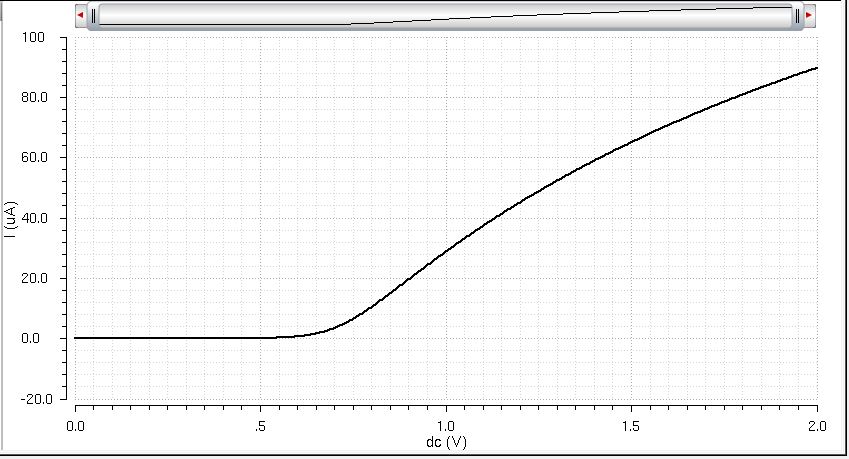
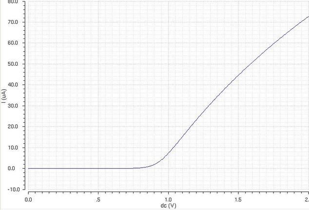
The following plot though was generated when VDS was held at a
constant 100mV and VGS again varied from 1 to 5V in 1V intervals.
This process was then repeated for the PMOS transistor.
The following schematic was created using the symbol created above.
The schematic produced the following plots for the IV curves with a varying VSD and constant VSD respectively.
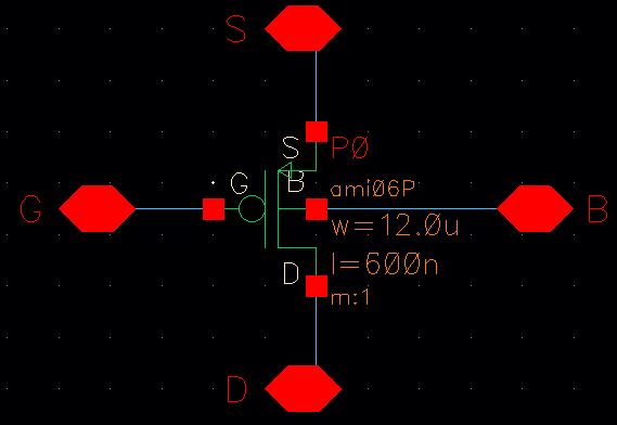
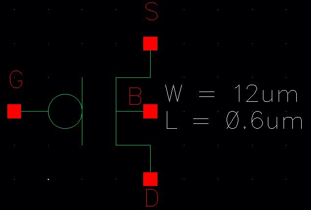
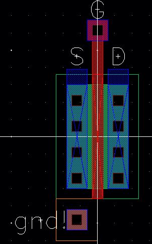
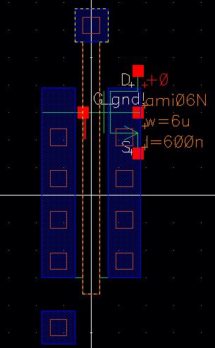
As
part of the prelab we were supposed to go through tutorial 2 and create
layouts and extracted views for both NMOS and PMOS devices. The
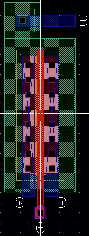
NMOS device can be seen in the following two pictures, where
this
picture is the layout view of the NMOS
and this picture is the etracted view.
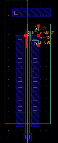
The PMOS device can be seen to be very similar in the following pictures
While performing the simulations,
we had to make sure the extracted views were being used before the
schematics, and in order to verify that we could see that this was the
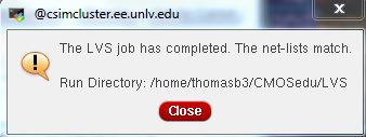
case based off the following picture. We also had to ensure the
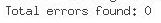
netlists matched while DRCing the layouts, which also had to succeed.
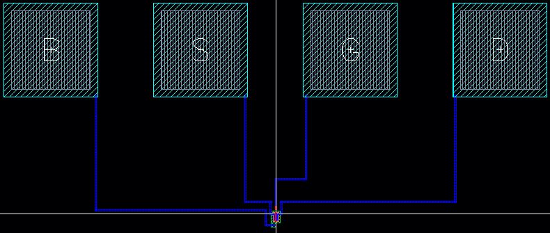
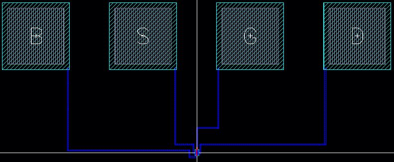
After
acquiring a general understanding of how the NMOS and PMOS devices are
laid out, it was time to turn them into a more useful form by attaching
them to bonding pads. This sort of layout is necessary when
connecting the transistors on the chip to circuitry off the chip. The following layouts were produced for the NMOS and PMOS transistors respectively.
NMOS:
PMOS: