Lab 2 - EE 421L
Brandon Thomas (email:thomasb3@unlv.nevada.edu)
Prelab Procedures:
- Download lab2.zip
to your desktop.
- This archive
contains a simulation example using an ideal 10-bit
Analog-to-Digital Converter (ADC) and Digital-to-Analog Converter
(DAC).
- Upload this zip file to the design
directory on the server that you are running Cadence from, e.g.,
Tutorial_1, CMOSedu, etc.
- Note that it's
assumed you are using the NCSU Cadence Design Kits.
- Unzip this directory and add, to your
cds.lib in the design directory, the following statement (assuming the
design directory is CMOSedu):
- DEFINE lab2 $HOME/CMOSedu/lab2
- Start Cadence from the design
directory.
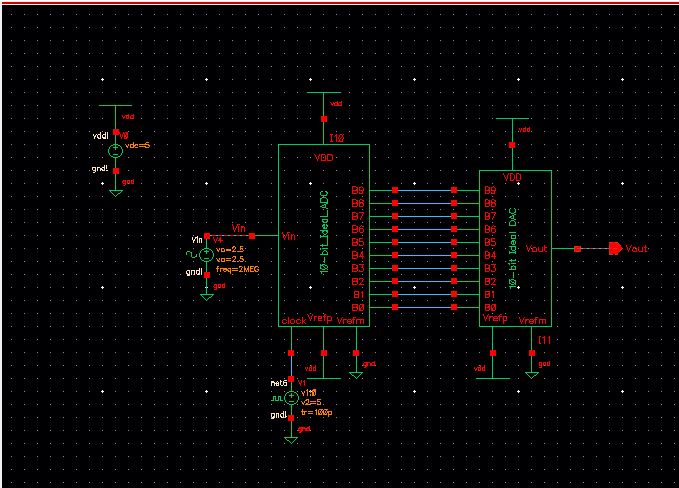
- Use the Library
Manager and navigate to the lab2 Library as seen below.
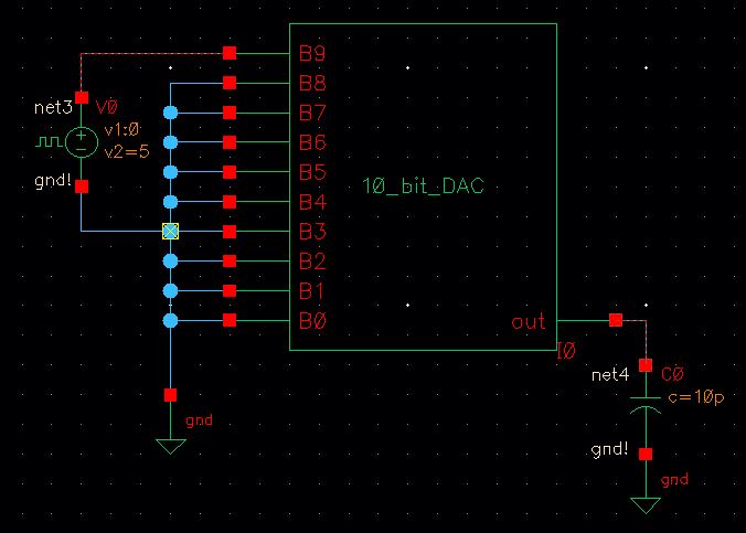
- Open the schematic view of the cell sim_Ideal_ADC_DAC.
- This cell contains
the ideal 10-bit ADC and DAC as seen below
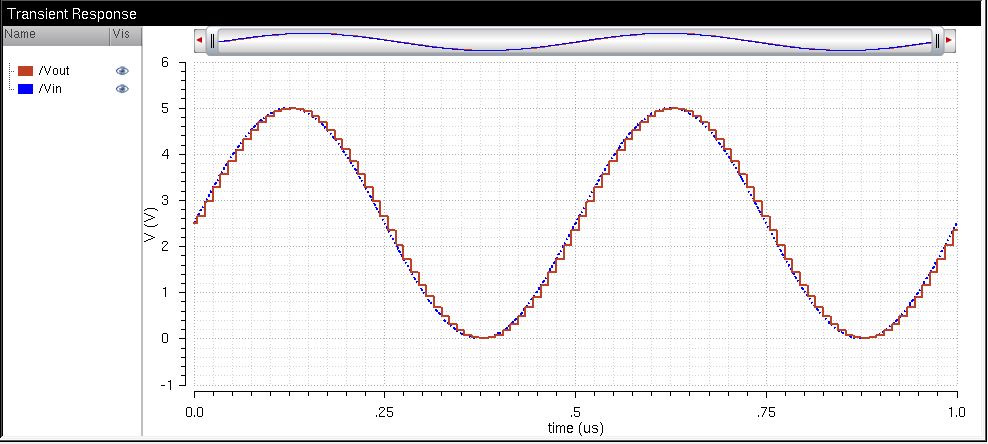
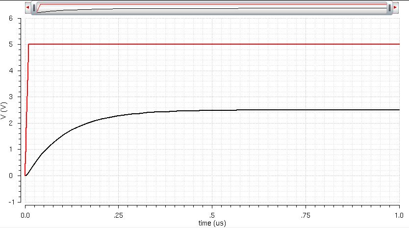
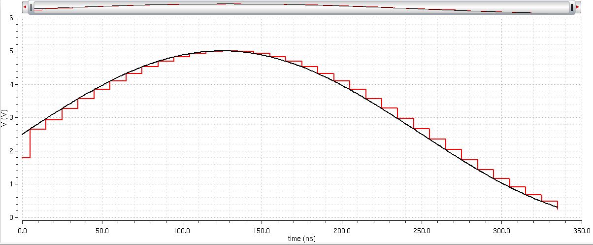
running a transient simulation of this schematic yields the following plot:
Lab:
After
simulating the premade circuit we had to build our own ideal 10-bit
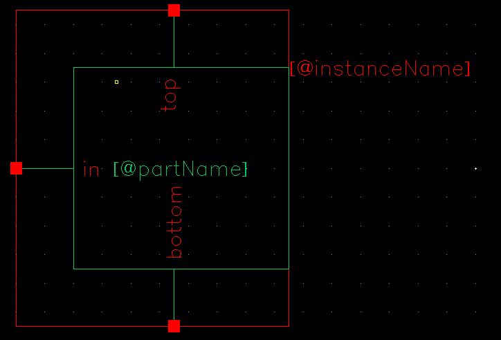
DAC. The first step was to create a 1-bit DAC, which can be seen
in the following screenshot, and use that as a building block within
the 10-bit DAC.
The schematic for the1-bit DAC was then turned into a symbol for simplified use in consturcting the 10-bit.
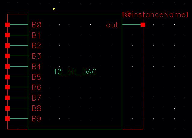
This was then used as the main building block for the 10-bit DAC,which was also turned into a symbol for convenient use.
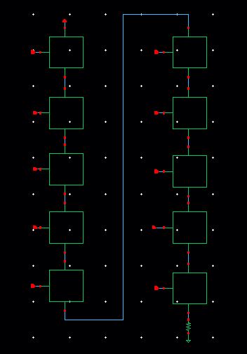
A
little issue arose when turning the 10-bit schematic into a symbol
because all of the pins flipped upside down which is the opposite way
they should be oriented. This would not have been a bad thing,
but wiring the outputs of the ADC to the inputs of the DAC would have
been a little bit messy. A simple verticle flip was the only
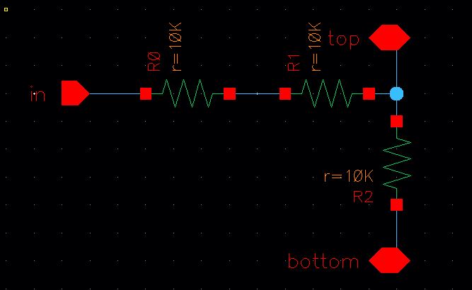
thing required to fix this, though. We then had to calculate the output
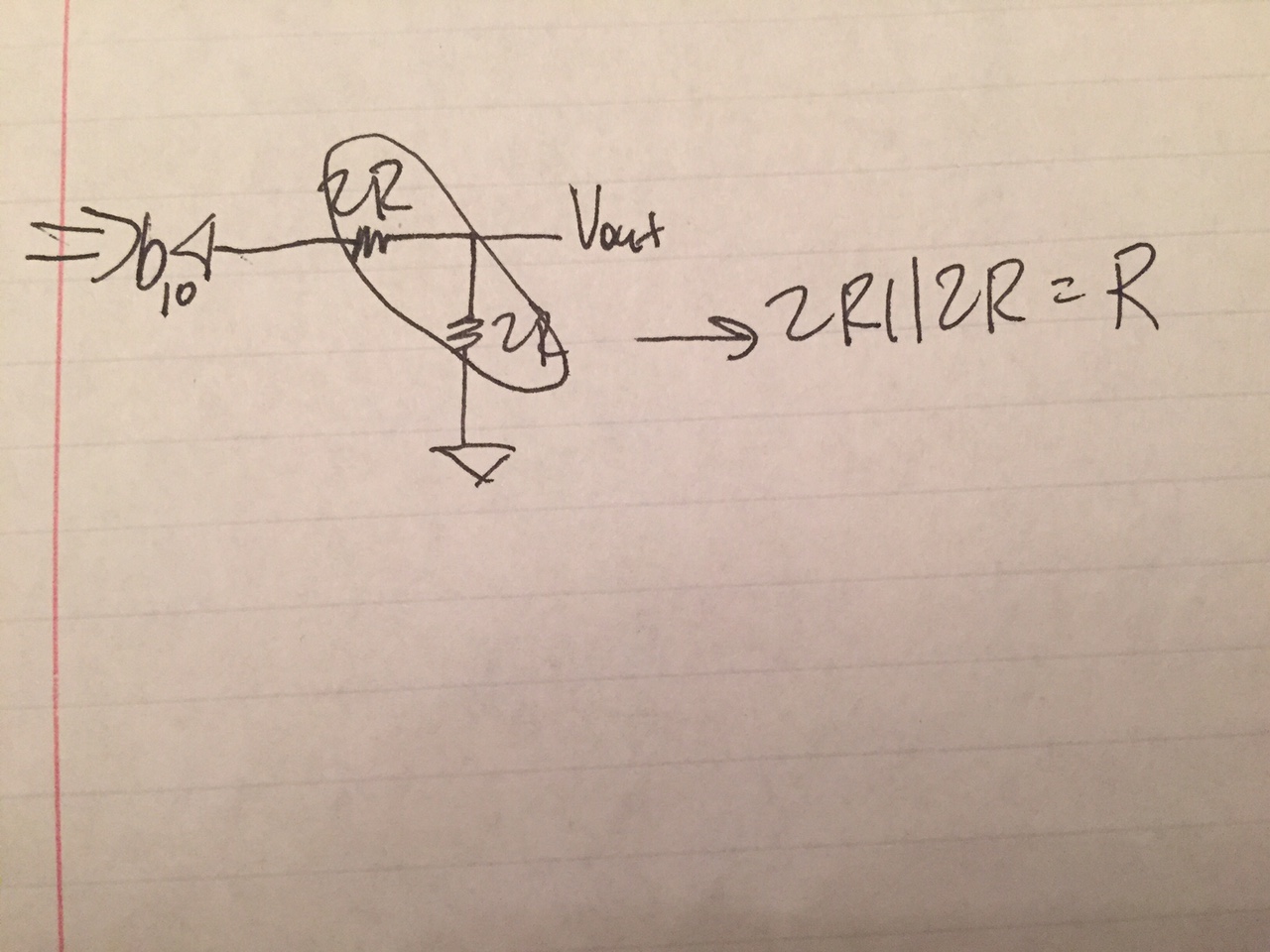
resistance of the ideal 10-bit DAC.
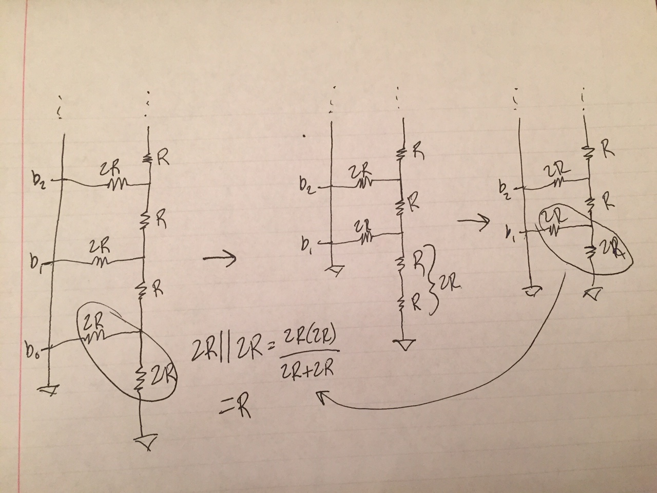
this process continues until the circuit is reduced to the following, where the overall output resistance is found to be R.
Using
this information we saw what the DAC would output to a specific input,
in order to see the delay of the circuit when an output capacitor of
10pFwas hooked up. This delay was estimated using the formula
0.7RC, which was found to be 70ns. This value is relatively close
based off of the simulation plot.
The DAC was then hooked up to the original ADC to DAC circuit in place of the DAC that was already there.
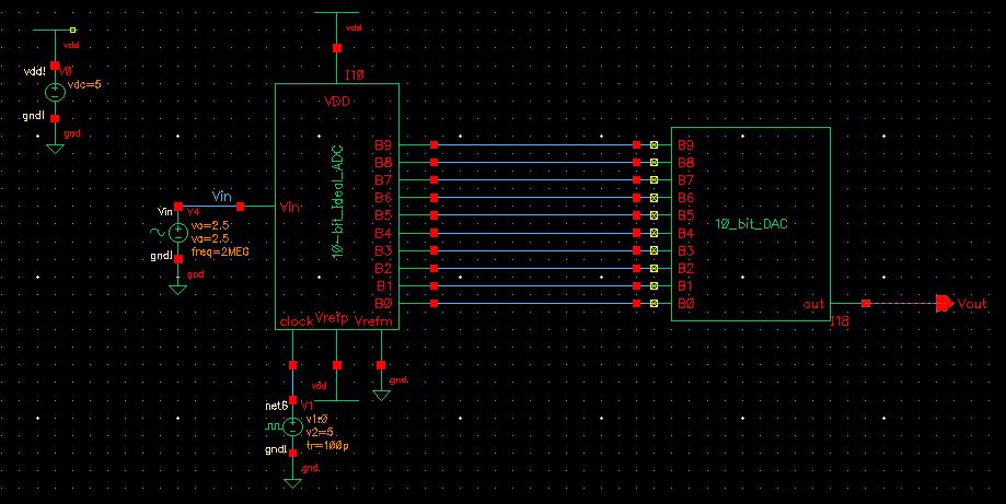
Another simulation was run, which produced the following plot:
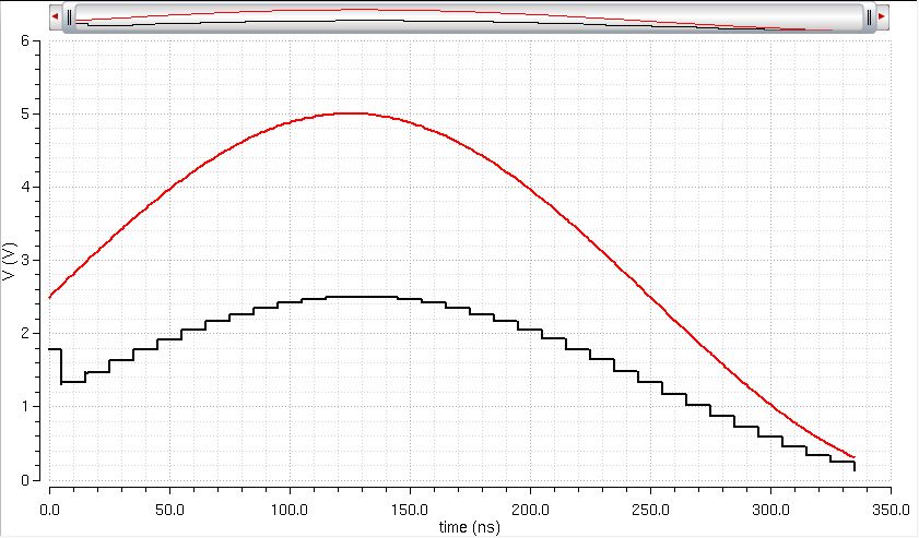
We
then had to test and see how different loads made the circuit output
change. The first load tested was a 10k resistor, which produced
the following output:
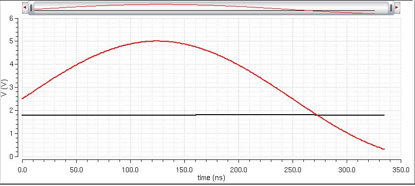
The
next test used a load capacitor, which produced the following output
plot (this output plot was the same output plot I got when hooking up
both the 10k resistor and the capacitor in parallelas loads).
After completing the lab, I backed everything up onto my desktop into a zip file, which I then emailed to myself.