Lab 4 - ECE 421L 

Authored by Stephanie Silic,

silics@unlv.nevada.edu

September 28th, 2015 


Lab 4 Description: 


This lab demonstrates  the IV (current vs. voltage) plots generated by NMOS and PMOS transistors, as well as how to construct the layout of these devices in Cadence.


Lab Report:


 Part 1 -- Generating schematics for simulations of IV characteristics for NMOS and PMOS transistors:
   
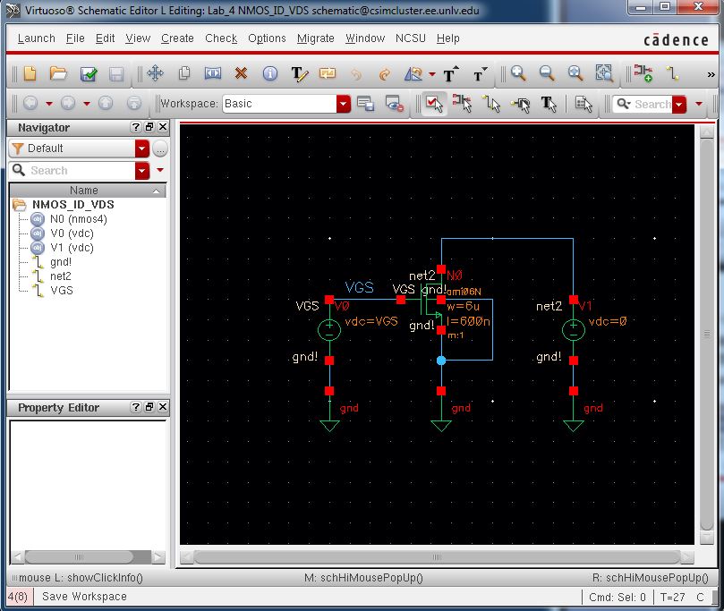
1) This first schematic is for simulating the ID vs. VDS curve of a 6u/600n (L/W) NMOS device, for VGS varying from 0 to 5V in 1V steps while VDS varies from 0 to 4V in 1mV steps.
   
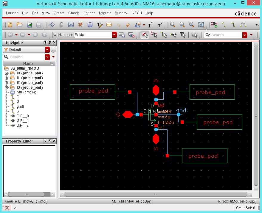
First, the schematic was drafted, using the nmos4 transistor. We need to ensure the body of the NMOS device is connected to ground, and that the voltage source on the left, V0, has a value of VGS, while the other source, VDS (V1 on the schematic), has a value of 0 so we can sweep it from 0 to 5V in the dc analysis phase.
 
http://cmosedu.com/jbaker/courses/ee421L/f15/students/silics/Lab4/NMOS_ID_VDS_sch.JPG
   
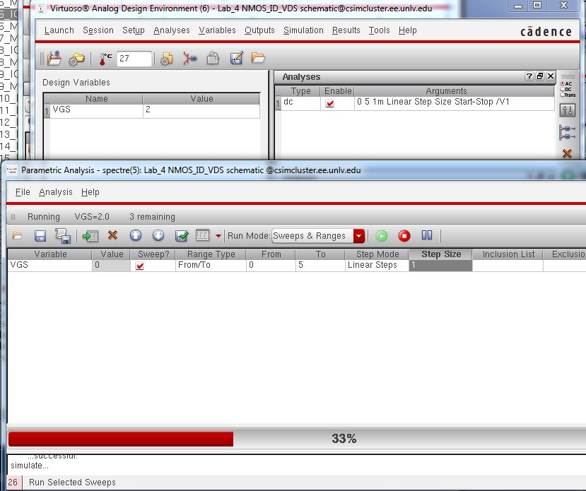
Next, the simulation parameters must be set up, first by loading a new state, then adding a new variable, VGS, from the tab Variables -> Edit and adding VGS with a value of 2. (VGS is going to vary, so this value could be anything.) Next, we select Analysis -> Choose, select the dc analysis, and sweep the component V1 (which is our VDS) from 0 to 5V in 1mV steps. Also, we must ensure that we are plotting the current ID, which can be selected on the schematic by clicking on the top node of the transistor. Finally, we select Tools -> Parametric Analysis and change VGS from 0 to 5V with Linear Steps of step size 1. Then we hit the green arrow in the Parametric Analysis window to run the analysis. The setup is as follows:
 
http://cmosedu.com/jbaker/courses/ee421L/f15/students/silics/Lab4/NMOS_ID_VDS_setup.JPG
 
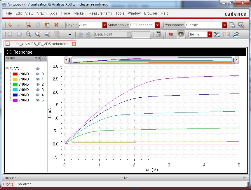
Finally, we get the following simulation results:
 
http://cmosedu.com/jbaker/courses/ee421L/f15/students/silics/Lab4/NMOS_ID_VDS_sim.JPG
   
2)  The second schematic is the same, but this time we hold VDS constant and vary only VGS.
 
http://cmosedu.com/jbaker/courses/ee421L/f15/students/silics/Lab4/NMOS_ID_VGS_sch.JPG
   
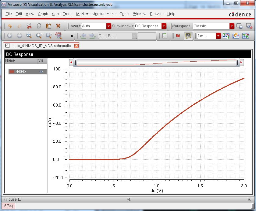
To simulate the ID vs. VGS curve, we can just choose the dc analysis and sweep the V0 parameter from 0 to 2V in 1mV steps:
 
http://cmosedu.com/jbaker/courses/ee421L/f15/students/silics/Lab4/NMOS_ID_VGS_setup.JPG
   
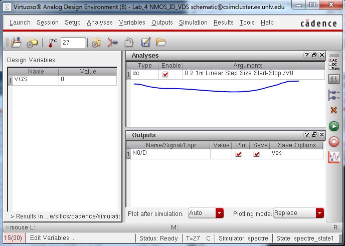
This will give the following plot:
 
http://cmosedu.com/jbaker/courses/ee421L/f15/students/silics/Lab4/NMOS_ID_VGS_sim.JPG
   
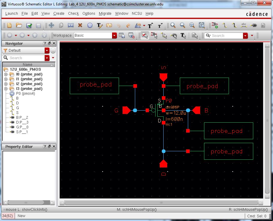
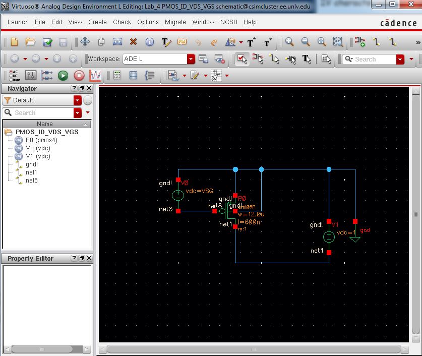
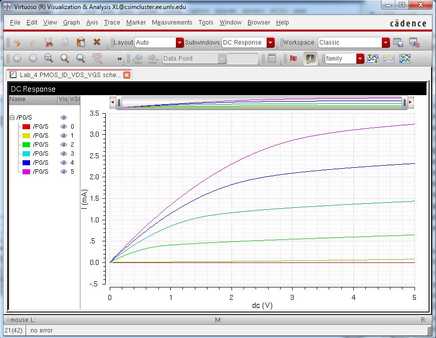
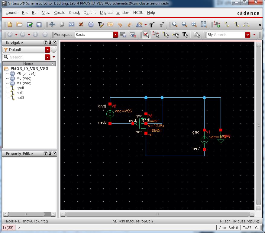
3) Thirdly, we want to make a schematic of a 12u/600n (L/W) PMOS transistor, to simulate the ID vs. VSD (not VDS, as in the NMOS device) curve.
 
The schematic is as follows, with the body connected to vdd! here, which is VSD.
 
http://cmosedu.com/jbaker/courses/ee421L/f15/students/silics/Lab4/PMOS_ID_VSD_sch.JPG
   
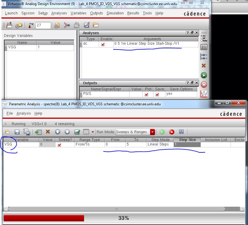
Now we again set up the parameters again, similar to what we did with the NMOS ID vs. VDS curve. We add the Variable VSG with a value of 1 (which doesn't matter), set VSD (V1 on the schematic) to go from 0 to 5V in the dc analysis window, and then we let VSG vary from 0 to 5 in 1V linear steps in the Parametric Analysis window:
 
http://cmosedu.com/jbaker/courses/ee421L/f15/students/silics/Lab4/PMOS_ID_VSD_setup.JPG
   
And the resulting plot is as follows:
   
http://cmosedu.com/jbaker/courses/ee421L/f15/students/silics/Lab4/PMOS_ID_VSD_sim.JPG
     
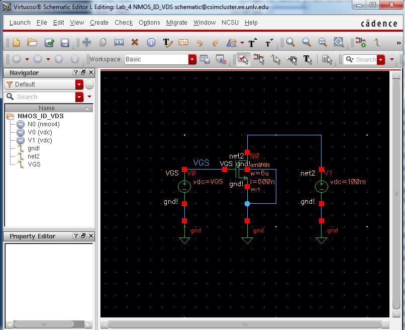
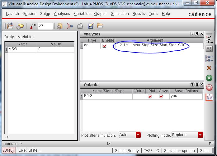
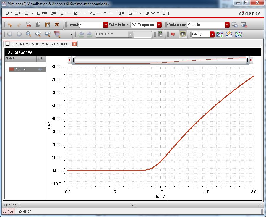
4) Fourthly and finally for this part of the lab, we use the same PMOS transistor schematic to simulate the ID vs. VSG curve, holding VSD at 100 mV.
 
The schematic:
 
http://cmosedu.com/jbaker/courses/ee421L/f15/students/silics/Lab4/PMOS_ID_VSG_sch.JPG
   
The setup only requires a dc analysis, sweeping VSG from 0 to 2V in 1mV steps:
   
http://cmosedu.com/jbaker/courses/ee421L/f15/students/silics/Lab4/PMOS_ID_VSG_setup.JPG
   
The resulting IV curve is as follows:
   
http://cmosedu.com/jbaker/courses/ee421L/f15/students/silics/Lab4/PMOS_ID_VSG_sim.JPG
   
Part 2 --
Layout of a 6u/600nm NMOS device and 12u/600nm PMOS device; connected to 4 probe pads:
 
  a) The layout of a 6u/600nm NMOS device. The device is connected to 4 probe pads and DRC the layout; the image below shows the entire layout and that it DRCs with no errors:
 
http://cmosedu.com/jbaker/courses/ee421L/f15/students/silics/Lab4/NMOS_layout-with-DRC.JPG


  The following image shows a closeup of the NMOS device, detailing its measurements and connection to the metal 3 wires which go to the probe pads:


  http://cmosedu.com/jbaker/courses/ee421L/f15/students/silics/Lab4/NMOS_layout-closeup.JPG


The schematic is then constructed, with 4 probe pads connected to the 4 terminals of the NMOS device: 


http://cmosedu.com/jbaker/courses/ee421L/f15/students/silics/Lab4/NMOS_schematic-for-LVS.JPG


And finally, after extracting the layout, we perform the LVS check. The following image shows the extracted view of the layout along with the LVS message that the net lists match:


http://cmosedu.com/jbaker/courses/ee421L/f15/students/silics/Lab4/NMOS_extracted-with-LVS.JPG


b) Now, for the PMOS device, the same procedure is repeated. The dimensions of the device are 12u (length) by .6u (width). We connect the 4 terminals of the device to 4 probe pads, and ensure it passes DRC:


http://cmosedu.com/jbaker/courses/ee421L/f15/students/silics/Lab4/PMOS_layout-with-DRC.JPG


A closeup of the PMOS layout shows how the metal 3 wires are connected through vias to the metal 1 of the device, and also its measurements: 

  http://cmosedu.com/jbaker/courses/ee421L/f15/students/silics/Lab4/PMOS_layout-closeup.JPG


Then, we use the schematic from Tutorial 2, and add 4 bond pads given in the lab4.zip directory. Once this is done, we can perform the LVS test with the extracted view of the layout.


http://cmosedu.com/jbaker/courses/ee421L/f15/students/silics/Lab4/PMOS_schematic-for-LVS.JPG


So once again,  the layout is extracted and we perform the LVS to ensure that the net-lists match:


http://cmosedu.com/jbaker/courses/ee421L/f15/students/silics/Lab4/PMOS_extracted-with-LVS.JPG


This concludes lab 4. 


My entire lab 4 Cadence directory can be found in Lab_4.zip


Return to listing of my labs