Project - EE 421L
Authored
by Shada Sharif,
sharifs@unlv.nevada.edu
9 November 2015
Lab Project Description:
- The
lab project is about fabricating a C5 process chip through MOSIS. The
chip will include an 8 bit UP/DOWN counter, NAND/NOR logic gates,
voltage divider, 25k and 10k resistors, 12u/6u and 6u/6u inverters, 31 stage ring oscillator, lastly NMOS and PMOS transistors.
Lab Project Report should include:
- Schematic and simulation of the 8bit UP/DOWN counter.
- Schematic and simulation of the 31-stage ring oscillator.
- Schematic and simulation of the NAND, and NOR gates.
- Schematic and simulation of the PMOS, and NMOS transistors.
- Schematic and simulation of the voltage divider.
- Schematic and simulation of the 25k, and 10k resistors.
NAND and NOR gates
- We first started making a NAND and a NOR gate. The schematic of the gates are shown below.
- After making the schematic we create a symbol in order to use it for simulation.
- The
following table shows the expected operation of the NAND and NOR gates,
and we see that the simulation matches the truth table.
- We
notice that each one of the gates have its own vdd power this is so
that when the layout is down we will not have power shared between the
circuits.
- In order to test the logic gates we connected a pulse
input to each one of the gate's inputs, and connected the noConn to the
output.
| A | B | | NAND | | NOR |
| 0 | 0 | | 1 | | 1 |
| 0 | 1 | | 1 | | 0 |
| 1 | 0 | | 1 | | 0 |
| 1 | 1 | | 0 | | 0 |
NAND
Inverter
- The second thing we do is an inverter, the inverter uses a 12u/0.6u PMOS and a 6u/0.6u NMOS.
- The inverter operates as the following:
- When
the input at the gate is 0, the NMOS is off and the PMOS is off when
forces the output to go to vdd so 0 input, results in 1 output.
- When
the input is 1, now the NMOS is on while the PMOS is off and this
causes the output to go to gnd that is a 1 input gives a 0 output.
- We again used a vdd pin for the inverter and not the supply net vdd.
- The following is the schematic of the inverter, followed by the symbol made for simulation purposes.
- In the simulation we connected a pulse input to the inverter input and we see how the output is inverted just like we expected.
- The truth table of the inverter is shown below:
PMOS and NMOS transistors
- Third part is making a 6u/0.6u PMOS and an NMOS.
- We
first make the schematic of the NMOS and the PMOS, as well as connect 4
pins/pads to each terminal (body,drain,source,gate), after the
schematic we create a symbol for simulation,
- Two simulation were done for the PMOS and the NMOS:
- One was varying VDS vs. ID, VSD vs. ID while varying VGS/VSG from 0 to 5V.
- Two was varying VGS vs, ID, VSG vs ID.
- We see through the simulation that the PMOS and NMOS are operating as expected.
NMOS
PMOS
8 Bit UP/DOWN Counter
- The
first part of making the counter is making a D flip flop with a clear
input. The DFF is edge sensitive meaning it changes the output state
with the high edge of the clock.
- Everytime the clock is
at the high edge the output follows the D input at that time so if the
input is 0 Q is 0 until the next high edge.
- The schematic of the DFF is shown below, and a symbol was made for the DFF.
- Transmission
gates were used in the schematic and the purpose was to hold the state
of the DFF for when the clock is changing everytime.
- In the schematic below we see two loops, when the CLK=0 T1 and T4
are on while T2 and T3 are off. So the input D goes and stays in loop
1. When the clock is changed to CLK=1 T2 and T3 are now on and the D
input is passed to loop 2 and we get Q and Q'. The second time
this happens the Q output was held in loop 2 until the clock changes
and that is how the DFF holds its state up to the next high edge in the
clock.
- The clear input was implemented using the nand gate
shown in the schematic below so that when the input is CLEAR is high
the input to the nand gate CLEAR_not is low and causes the output to go
to zero.
- In the simulation below we see also how the CLEAR
input is also working where it dominates when it is high and regardless
of the D input the output sets to 0.
| 1 | 0 | 0 |
| 1 | 0 | 1 |
| 1 | 1 | 0 |
| 1 | 1 | 1 |
| 0 | 0 | 0 |
| 0 | 0 | 1 |
| 0 | 1 | 0 |
| 0 | 1 | 1 |
| 1 | 0 | 0 |
| 1 | 0 | 1 |
- We
first start by making a 1 bit up/down counter, using the table
constructed above of a 3 bits as an example we see that the first bit
changes every cycle, while the second bit changes every other cycle.
Which is why we have the Q or Q' depending if we want to count up or
down fed to the clock of the second DFF and not all the DFF connected
to a synchronous clock.
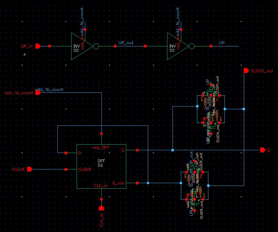
- In order to control the counter to
either count up or down we used transmission gates again with an input
called UP_in. When UP_in is high the counter counts up since Q is the
output of the DFF, and through the bottom transmission gate Q_not is
fed into the clock of the second DFF. When UP_in is low the upper
tranmission gate is on and while the output is Q it is also fed into
the clock of the second DFF.
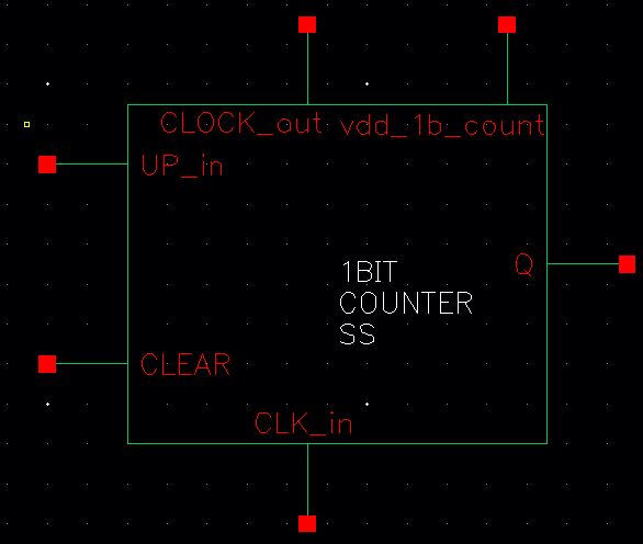
- The schematic of the 1 bit
counter is shown below, a symbol of the schematic was made so that it
is used later for the 8 bit counter.
 |  |
- Now
we start making the 8 bit up/down counter, and it is done using arrays
and bus wires. We use the array <0:7> that represents 8 bits, and
we connect the wires in the same fashion we did for the 31 stage ring
oscillator that will be shown later.
- The schematic of the 8 bit up/down counter is shown below, and a symbol was made for the simulation.
- We
conduct several simulations in order to check that the 8 bit counter is
operating correctly and can count up or down and that the Clear is also
working.
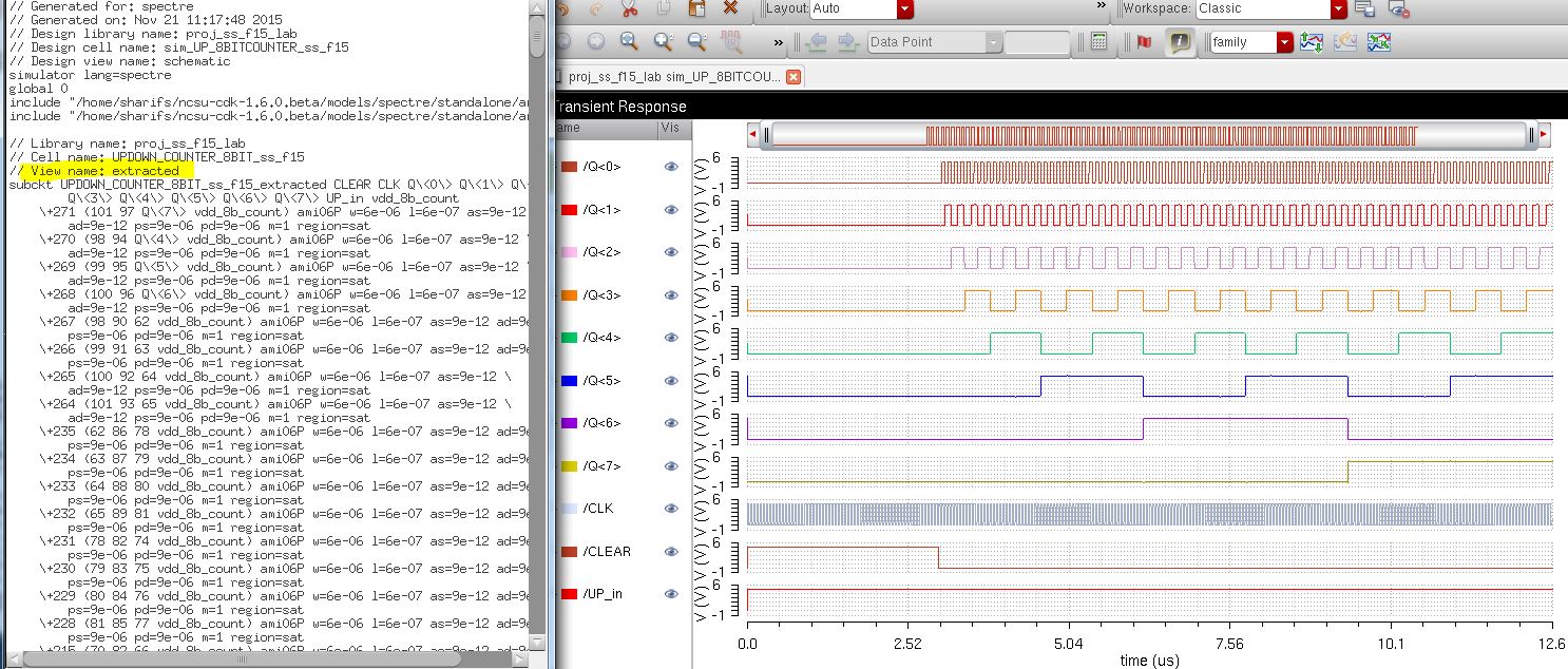
- The
first simulation is counting up without a clear input, we noticed that
the clock signal frequency had to be increased so that all the Q
<0:7> outputs are counting.
- The UP_in was high so that the counter can count up.
- The second simulation was counting down, and this was done using the same exact
schematic from above but changing the UP_in to low so that the counter
counts down.
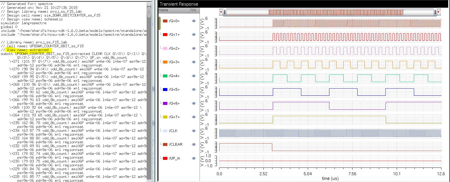
- We could see how in the simulation for example Q<7> starts at 1 while previously while counting up it started at 0.
- The
third simulation was the same as the first one but having a clear input
to test if it works. For clear to be active we need to have it high so
we changed it to be 5V, and we could see how the Q<0:7> outputs
are low/0 during the time clear is high.
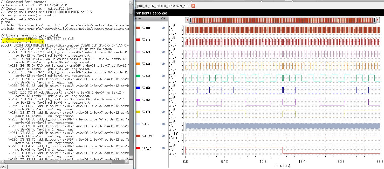
- The
last simulation test was to have the UP_in switch from 1 to 0 so while
the counter is counting up, UP_in switches and the counter starts to
count down.
25k Resistor
- We start by instantiating a resistor and changing the value to 25k ohms, and then we create a symbol for the 25k resistor.
- We use two pads for the resistor, as seen below one pin is called L and the other is called R.
- The
simulation of the resistor is shown below, we dc sweep the input and
plot the output to see a linear change just as we would expect from
resistor plot.
- We also did the same for the 10k ohms resistor that will be used later for the voltage divider.
Voltage Divider
- For
the voltage divider we use the two resistor symbols made previously and
create the voltage divider as shown below in the schematic.
- We
add an extra pin for the output of the divider, as well as a ground pin
for the common ground pad that will be used later in the project.
- We then create a symbol of the schematic, and use it for simulation.
- For simulation we use a dc input and test a dc sweep of the divider and a transient analysis.
- Shown below we see that the simulation results match the calculation of the voltage divider.
Vout=(10k/(10k+25k))*Vin
Vout=(10k/35k)*Vin
Vout=0.2857*Vin
Vout=0.2857*5V=1.43V
31-Stage Ring Oscillator
- The
last thing was about making a 31-stage ring oscillator, the oscillator
consists of 31 inverters connected in series as well as the output of
the last inverter connected back to the input of the first
inverter.
- Instead of making the oscillator using an actual 31 inverters, we used bus wires and created an array of the inverter.
- The array consisted of 31 inverters, and it was done using the brackets < >.
- The schematic of the oscillator is shown below and then a symbol was made for the simulation.
- Now
we test the oscillator driving a 20pF load, and we notice that the load
is too large for the oscillator and the output is not correct since the
oscillator cannot supply enough current for the load.
- Thus, we added a buffer at the output of the oscillator, which is having two inverters connected in series.
- The
first inverter was multiplied by 8 and that causes the width to be
multiplied by 8 which means more current is supplied, and the second
inverter was multiplied by 16, but we noticed that the output was still
not fully correct, thus we changed the second multiplier to 64.
- From
the simulation below we see that the output is almost as identical to
the simulation of the oscillator without the load. Increasing the
widths of the inverters will cause the output to look more similar to
the oscillator output without load.
Layout for the schematics
- All the layouts below will have the extracted version as well as the DRC showing no error and the LVS matching the schematic.
- The
extracted was used for simulation to prove the functionality of the
layout and to show that the simululation is for the extracted the
output log was displayed next to the simulation.
NAND and NOR gates
- Below
are the layout of the NAND gate, the extracted view, as well as the DRC
with no error and the LVS matching the schematic above.
- The simulation of the extracted was made to make sure that the layout gives the same results as the schematic.
NAND
NOR
Inverter
NMOS and PMOS
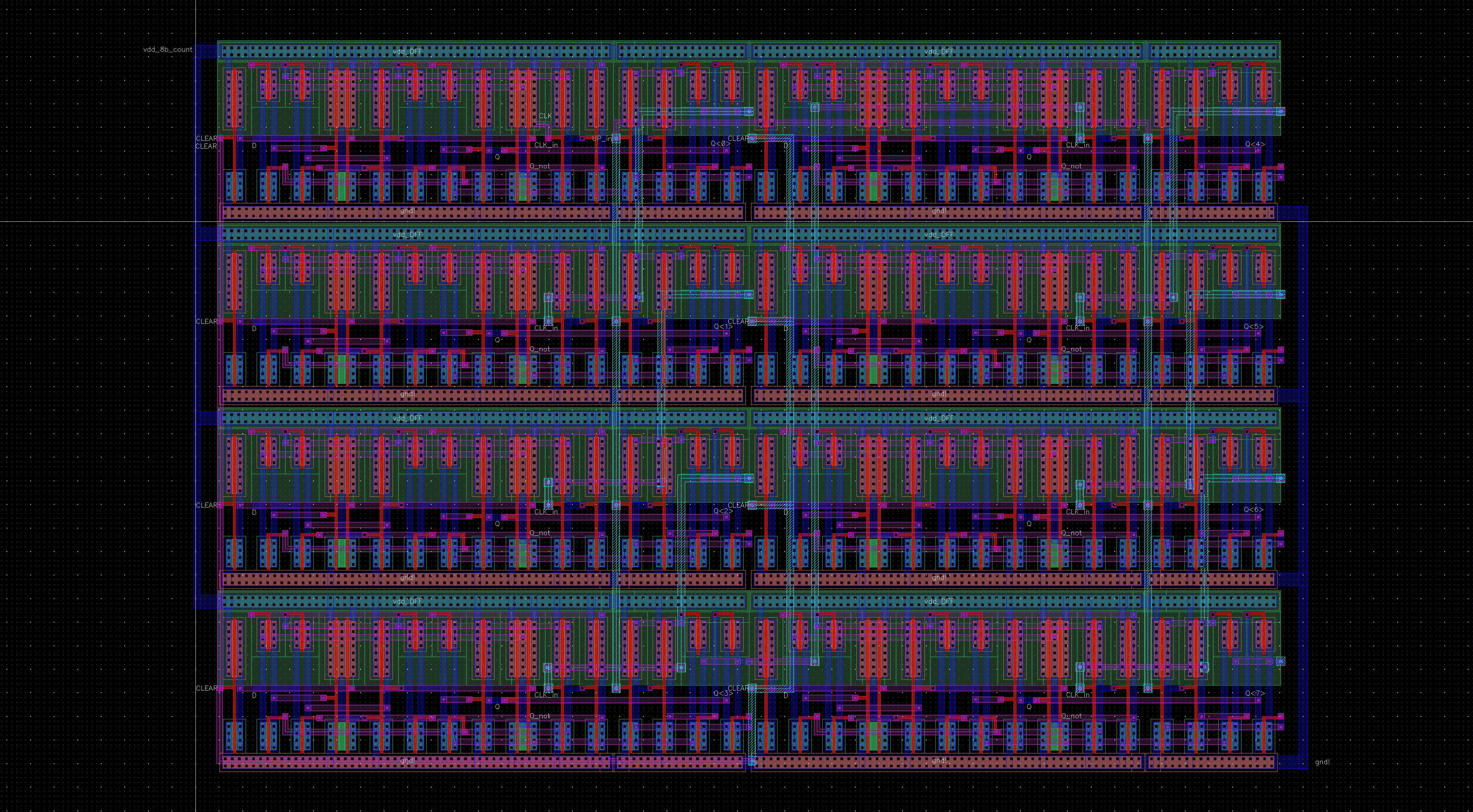
8 Bit UP/DOWN Counter
DFF
1 Bit Counter
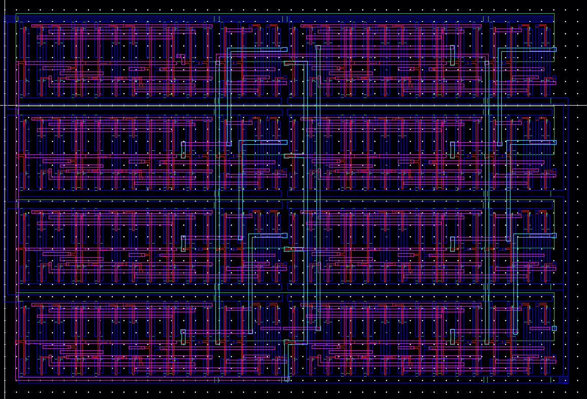
8 Bit UP/DOWN Counter
Click on the image to enlarge
 |
 |
 
|
Counting down with a Clear
|
Counting Up with a Clear
|
Counting UP and Down
 |
10k and 25k resistors
Voltage Divider
31 Ring Oscillator
Oscillator without a buffer
Oscillator with buffer
Backup
- The back of the entire lab was done through Dropbox as seen below.
Lab Project zip file
Return to EE 421L Labs
