Lab 2 - EE 421L
Authored
by Emmanuel Sanchez,
Email: sanch512@unlv.nevada.edu
8/30/2015
Lab
description:
The purpose of this lab is to implement and simulate a 10-bit Digital-to-Analog-Converter (DAC).
10-bit DAC Simulation:
Schematic of 10-bit ADC followed by 10-bit DAC.
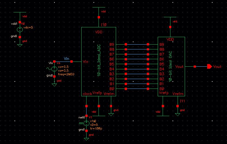
Input Signal: 2.5V amplitude, 2.5V offset
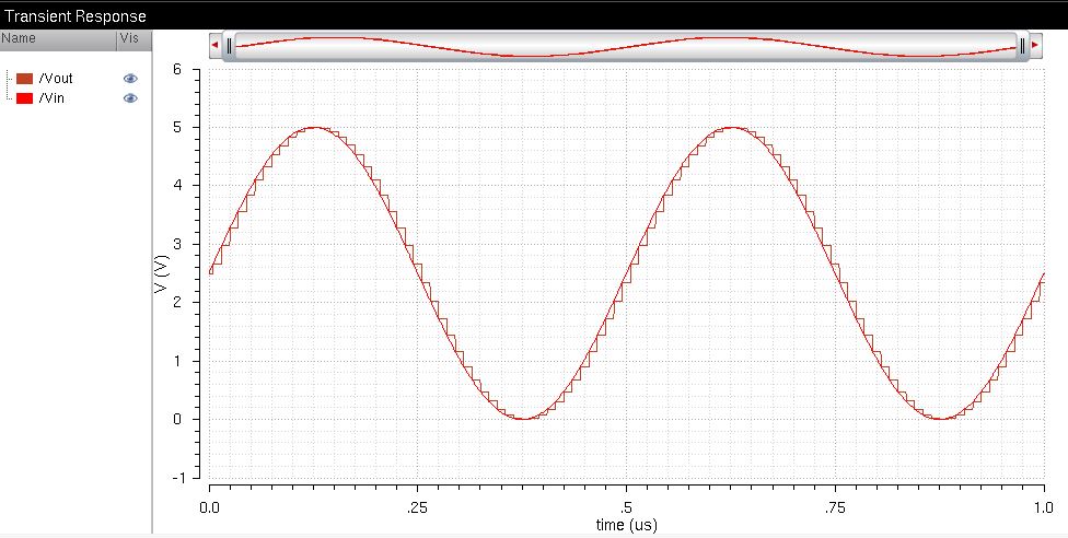
The Least Significant Bit (LSB)
The LSB determines the resolution of the digital
signal. The smaller the LSB, the higher the resolution, and the closer
the digital signal will be to the original analog signal.
The LSB is determined by:
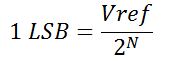
Where Vref is the highest digital value that can be represented, and N is the number of bits in the ADC.
In this lab, the reference voltage (Vref) is 5V. Solving the equation for LSB we have:
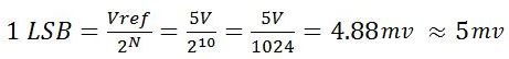
This means that the smallest change that can be detected in the analog input signal is 5mV.
More Simulations
Now
that we know that the LSB in this lab is 5mV, we can run a few more
simulations with smaller input signals to show how the digital
signal can only respond to changes of 5mV or greater.
Modifying the input signal to see the effects on the output signal.
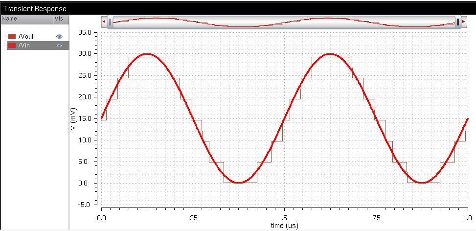
EXAMPLE 1:
Input signal = 15mV amplitude, 15mV offset
In
the following image, we can see how the digital signal can only respond
to changes in the input signal that are greater than 5mV.
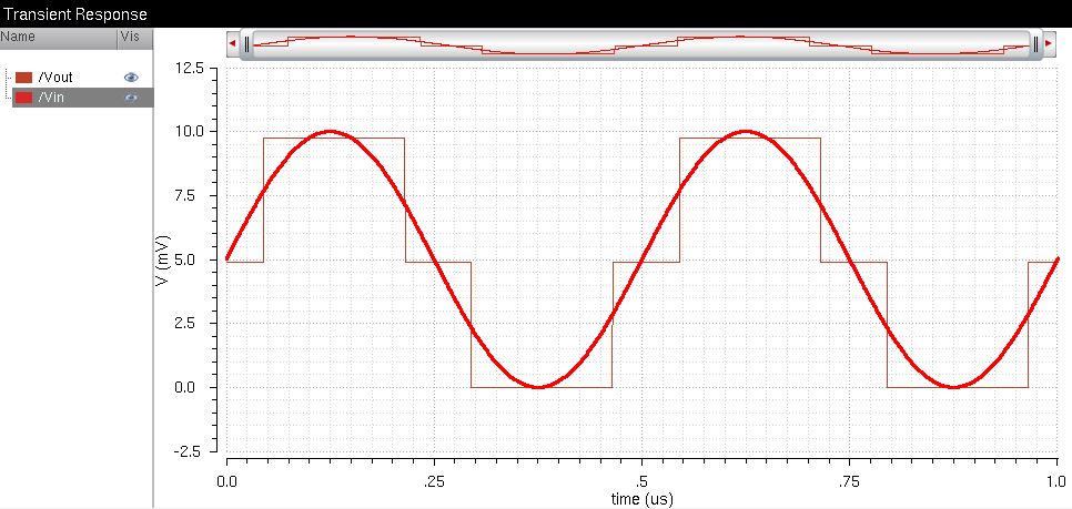
EXAMPLE 2:
Input signal = 5mV amplitude, 5mV offset
Again, the following image shows how the digital signal only responds to changes in the input signal that are greater than 5mV.
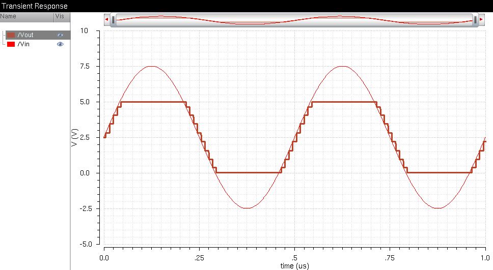
Input Signal Limitations
The
output of the ADC can only represent values ranging from Vrefm (0V) to
Vrefp (5V), so the analog input signal must be between these
boundaries. The following image shows an
input signal that is not within 5V and 0V. We can see the the digital
signal was only able to reach a maximum of 5V and a minimum of 0V.
Postlab
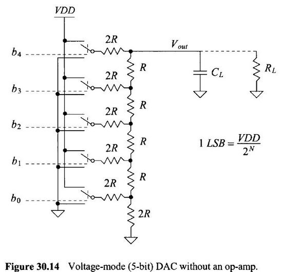
Use 10k n-well resistors to implement the 10-bit DAC found on figure 30.14 in the CMOS book.
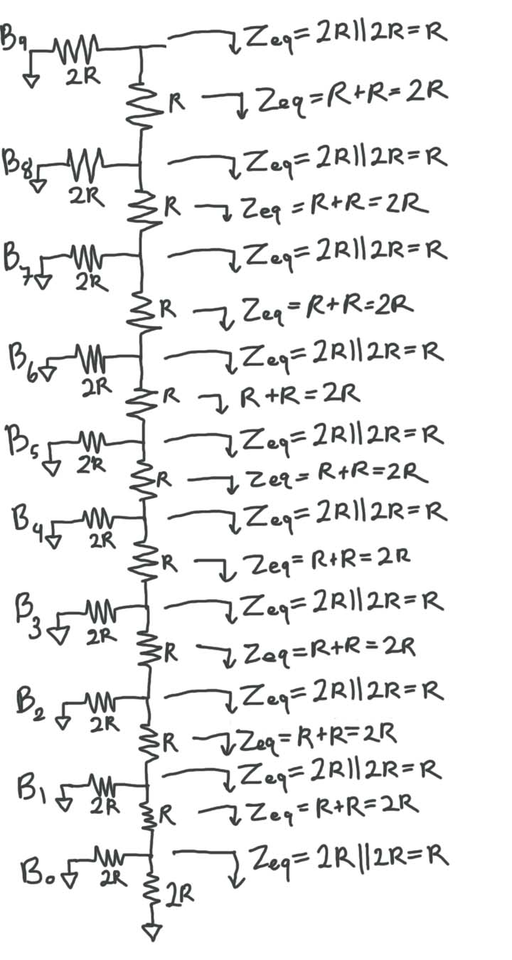
The output resistance of the DAC is found by combining the R-2R resistors in parallel and series like seen below.
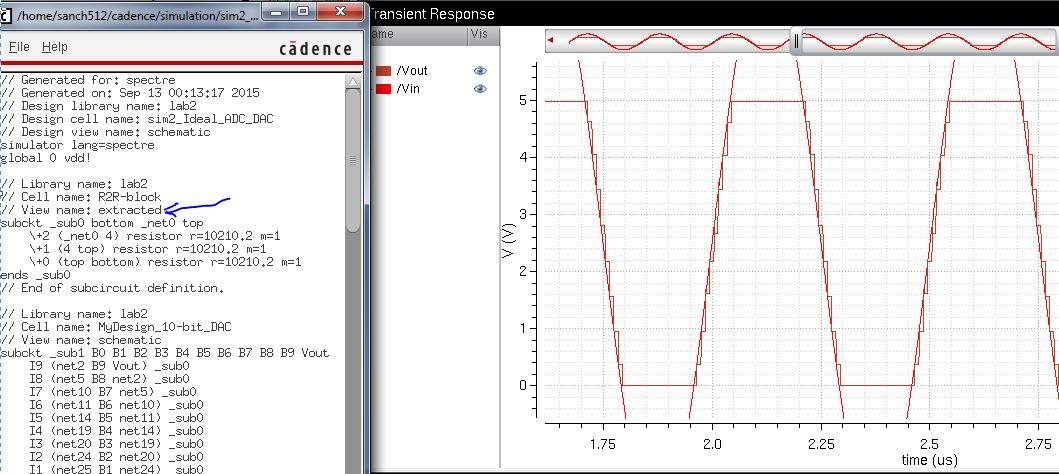
The
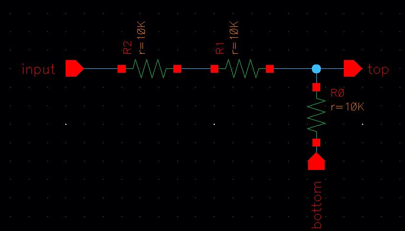
following image shows the schemactic of the R-2R blocks that will be
used in the DAC schematic. The 20k resistor was implemented using two
10k resistors in series.
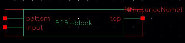
From the R-2R schematic, I created a symbol.
The layout for the R-2R block is seen below.
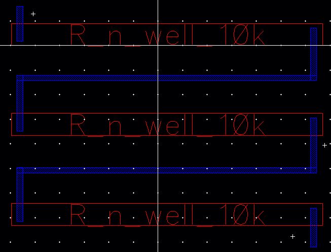
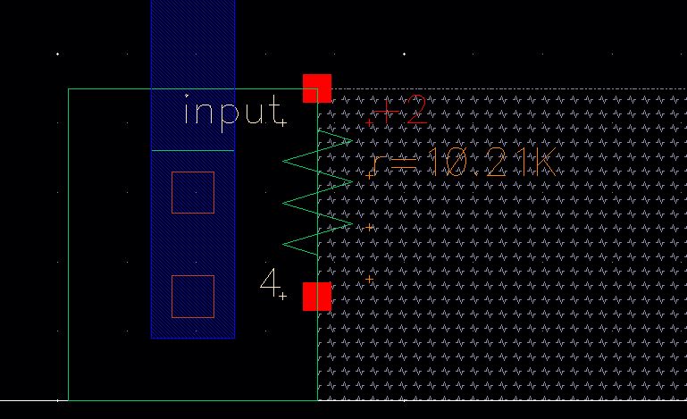
We can see in the extracted view that the n-well resistors are actually 10.21k and not exactly 10k as intended.
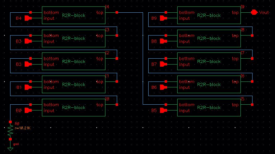
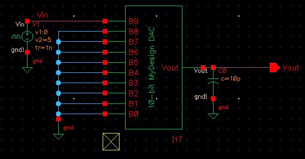
Using the symbol from the R-2R block, I built the schematic for the DAC.
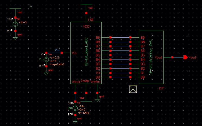
After
copying and modyfing the symbol from Ideal_10-bit_DAC, my DAC symbol
now has the same footprint as the Ideal_10-bit_DAC. The following
schematic shows the my DAC replacing the DAC from the original
schematic.
Running a simulation with the extracted layout shows that the circuit is still functioning as expected.
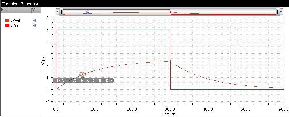
If
we put a 10pF load at the output of my DAC and a pulse at the input of B9, the delay should be 0.7RC
where R=10k (the output resistance of the DAC) and C=10pF (the
capacitive load).
This yields: 0.7(10*10^3)(10*10^-12) = 0.7(10*10^-9) = 70ns
Running the simulation confirms that the delay of my DAC with a 10pF load is about 70ns.
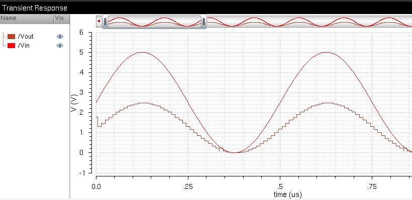
Now we test the DAC with resistive loads of 1k, 10k, and 100k.
Using a 1k load:
We can see the circuit acts as a voltage divider and the highest value for the output is:
5V[Rload/(Rload+Routput_of_DAC)] = 5[1k/(1k +10k)] = 454mV
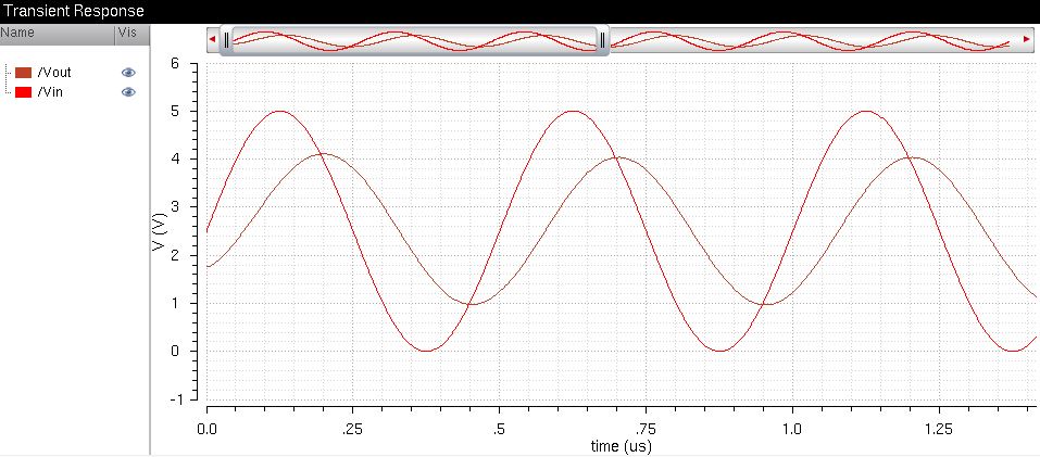
Using a 10k load:
Again,
we see the circuit acts as a voltage divider and the highest value for
the output is exactly half of the input, because both the load and the
output resistance of the DAC are 10k.
Using a 100k load:
In
this simulation we see that the load does not have a big effect on the
output because the load resistor has a high value compared to the
output impedance of the DAC.
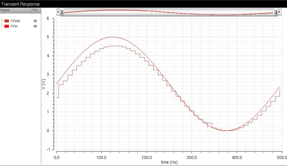
Now we simulate the DAC using a 10pF load.
In this simulation we see that the capacitive load affects the amplitude and phase of the output signal (lagging).
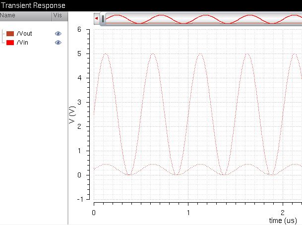
Finally, we simulate the DAC with an RC load (R=10k & C=10pF):
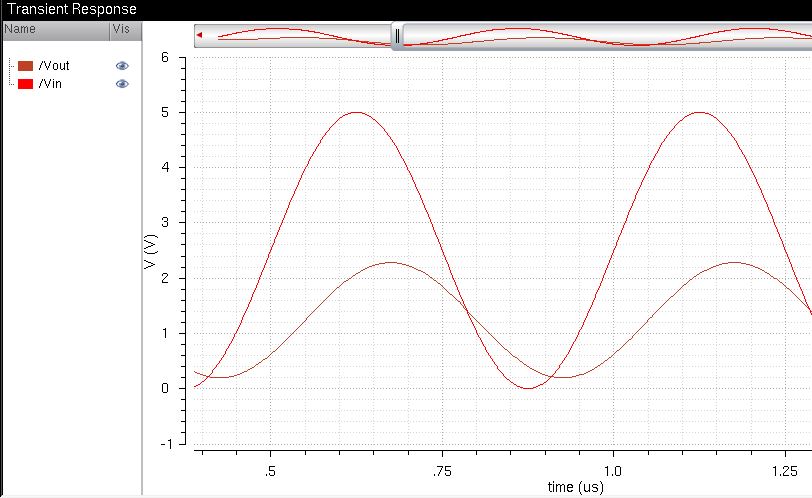
Here we see that the 10k
resistor prevents the output from reaching values above half of the
input signal (as discussed earlier). And the capacitor affects the
phase of the output (lagging).
In
real circuits, the switches seen in figure 30.14 are implemented with
MOSFETS. If the resistance of the switches is not small compared to R,
the output impedance of the circuit will increase, causing the output
voltage to decrease and the time delay to increase.
Return to EE421L Labs