Lab 2 - EE 421L
Authored
by Russ Prado,
prador@unlv.nevada.edu
09/14/2015
Pre-Lab
Lab
description:
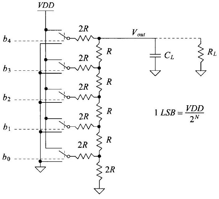
Use the n-well resistors to implement a 10-bit DAC
Design of a 10-Bit Digital-to-Analog Convertor(DAC)
Step 1:
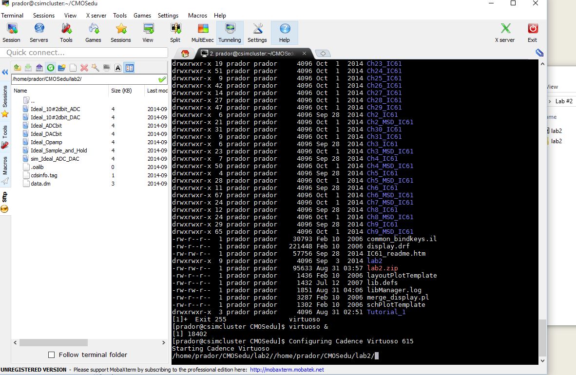
Download and unzip the schematic files, lab2.zip, onto Cadence
Step 2:
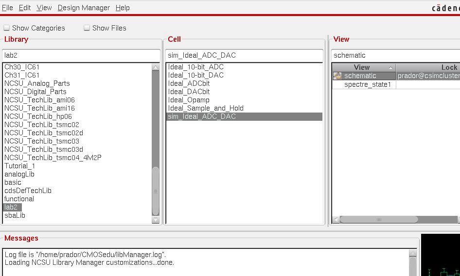
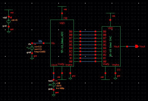
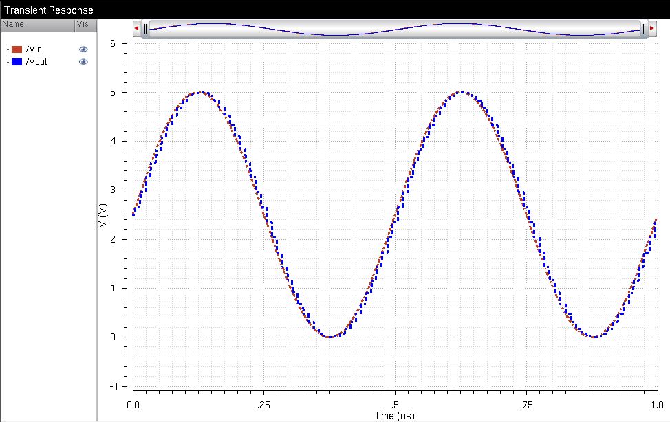
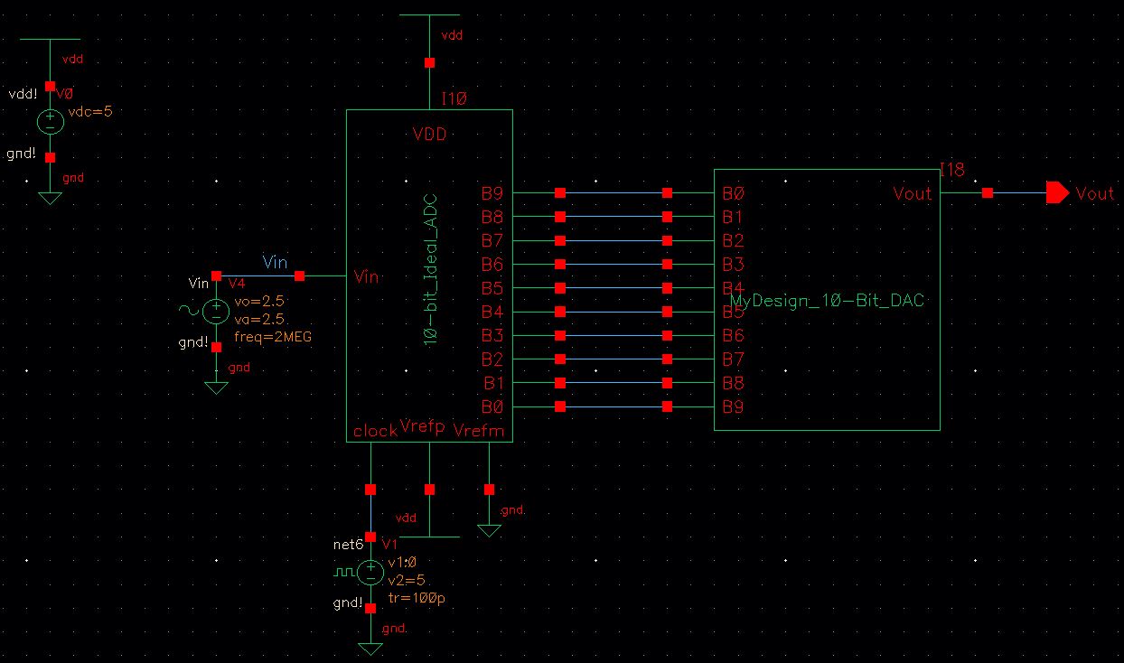
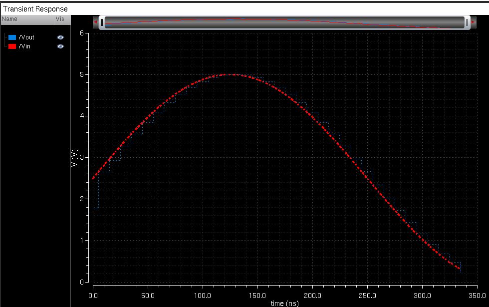
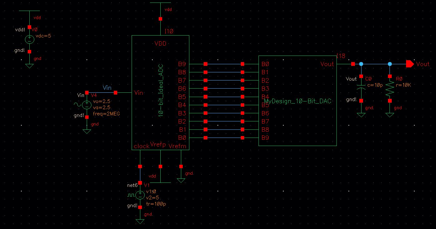
Open the Ideal ADC-DAC schematic, then run a transient analysis for 1us
Post-Lab
Step 3:
This part of the lab will be using the following layout but using 10-Bits instead.
Step 4:
Create a schematic of of the following voltage divider which will be title, "2R_Res".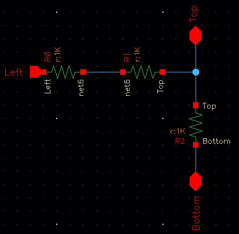
Step 5:
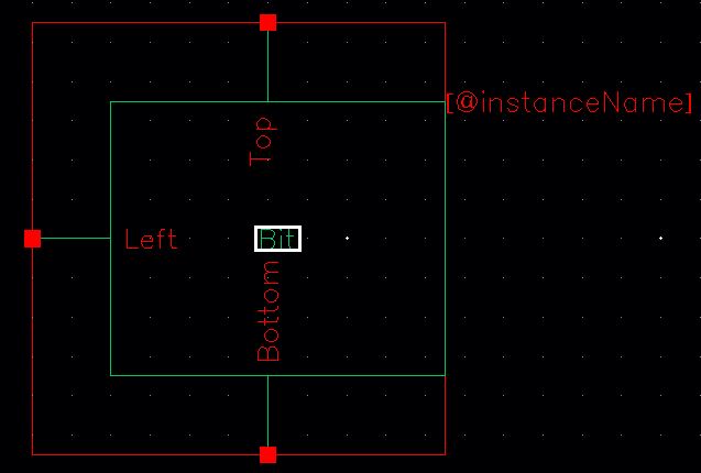
Create a symbol using the "2R_Res" schematic using the Create>Cellview>from Cellview.
Step 6:
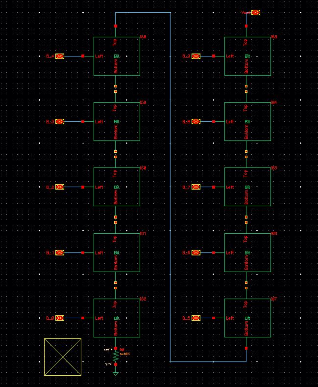
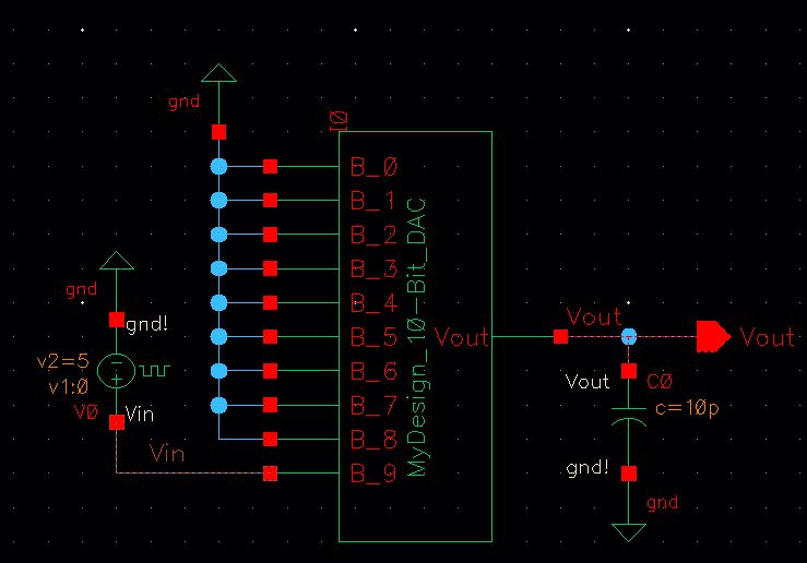
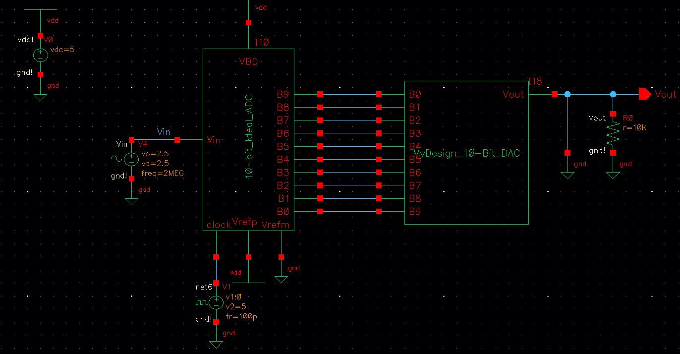
Now we will create our design of the 10-Bit DAC using the 2R_Res symbol we created. Make a copy of the Ideal_10-bit_DAC
and rename it to "MyDesign_10-Bit_DAC". Delete everything in this new
schematic. Place 10 of the 2R_Res symbols in series. Don't forget to
add a 10k resistor and ground on one end of the series and the an
output pin on the other end. Finally Check & Save.
Part 7:
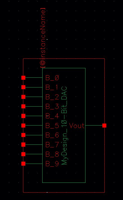
Open the symbol of MyDesign_10-Bit_DAC. Then delete the VDD, Vrefm, and Vrefp.
Part 8:
Test the your 10-Bit DAC design by putting a 5V input onto B_9 while the other DAC inputs are grounded.
Part 9:
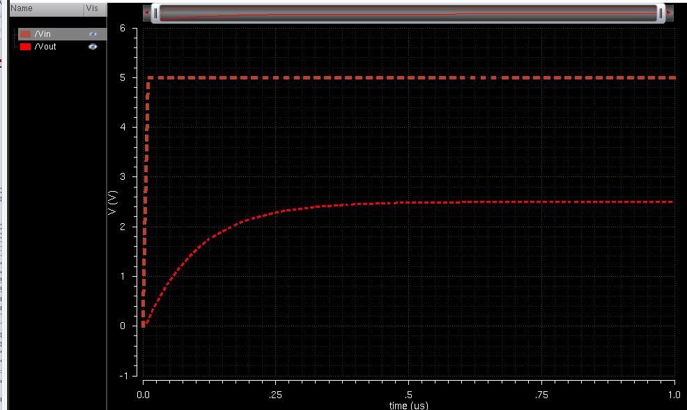
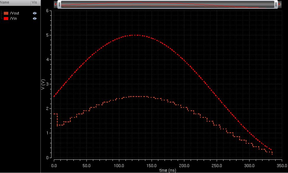
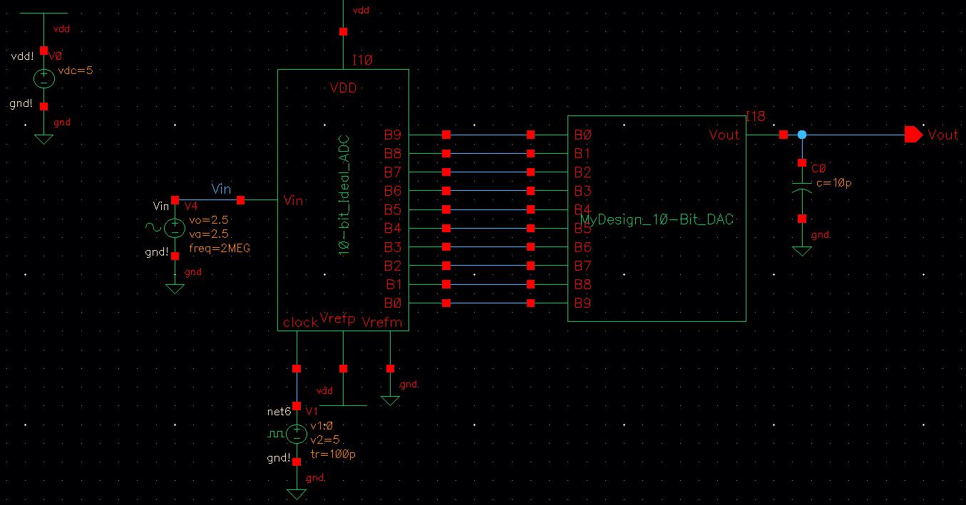
Create a copy of of sim_Ideal_ADC_DAC and rename it as "sim2_Ideal_ADC_DAC". Open its schematic and replace the current DAC with MyDesign_10-Bit_DAC. Then run the Transient response. Run this schematic with no load, R, C, and RC:
I. No Load
II. 10k Resistor
III. 10pF Capacitor
IV. 10k Resistor and 10pF Capacitor
Part 10:
With the files on my desktop, I compress them into a zip file and send it to my email to keep a back-up.
Return