Lab 4 - ECE 421L
Co Nguyen
9/24/2015
Lab
description:
IV characteristics and layout of NMOS and PMOS devices in ON's C5 Process
This lab is create schematics, layouts, and simulation of NMOS and PMOS devices in the C5 Process
The schematics and simulations of NMOS:
- ID
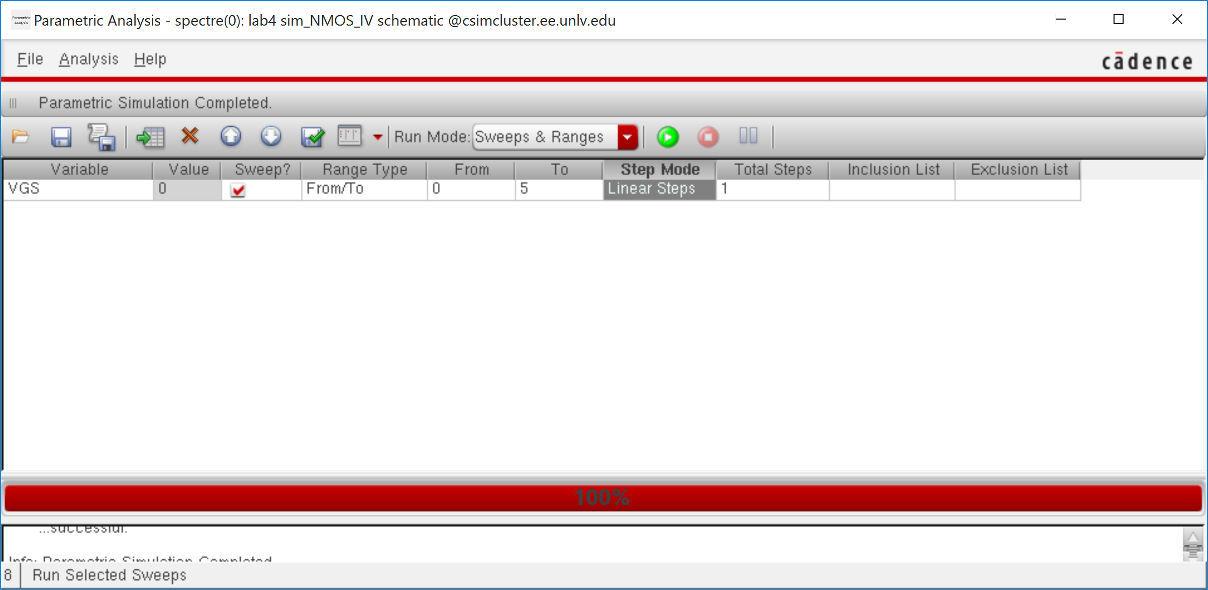
vs. VDS of an NMOS device for VGS varying from 0 to 5 V in 1 V steps
while VDS varies from 0 to 5 V in 1 mV steps (W/L= 6u/600n)
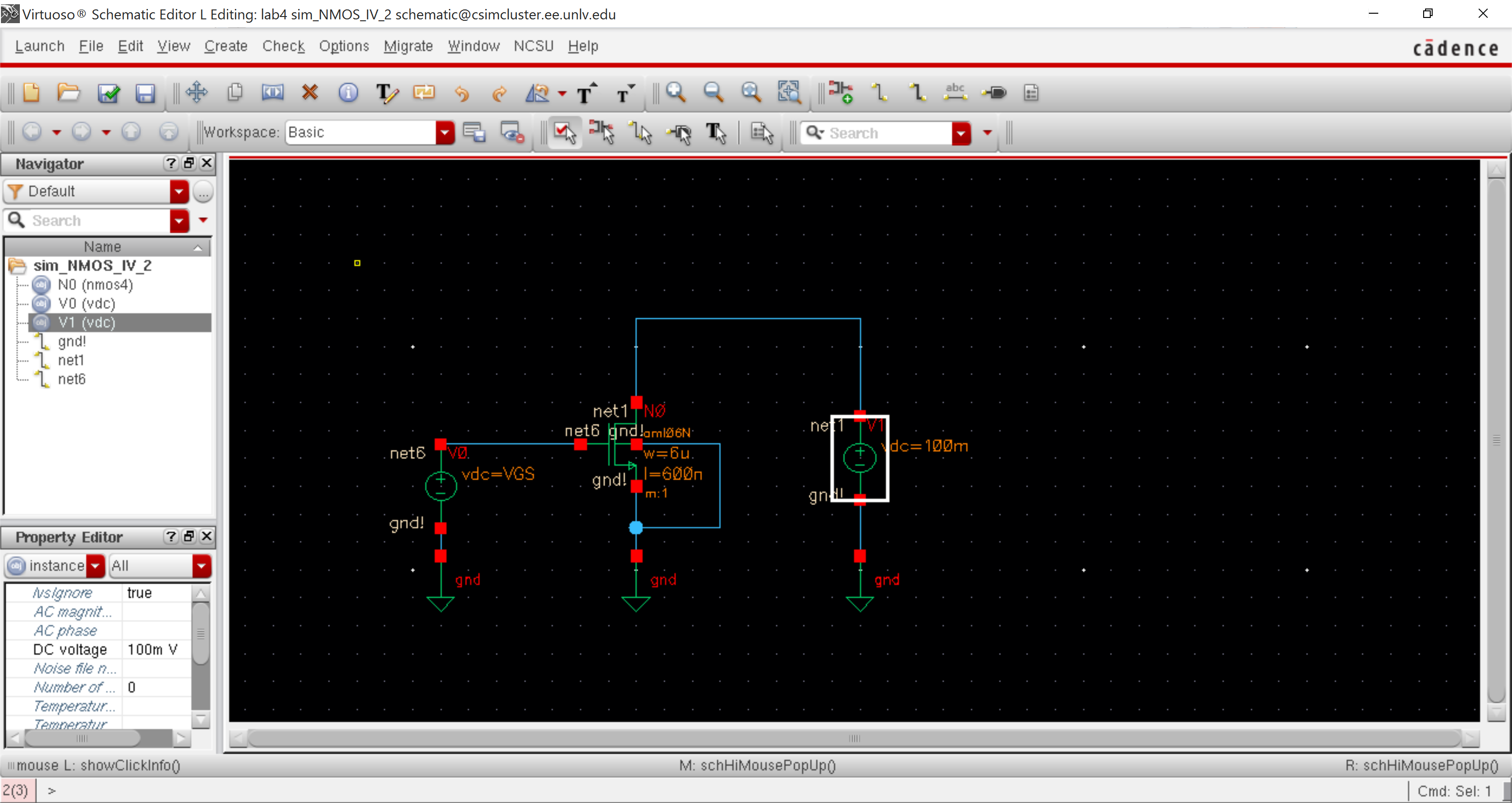
I find NMOS schematic device by hit key 'I' to bring the Library: "NSCU_Analog_Parts" ->N_trarnsistors-> nmos4.
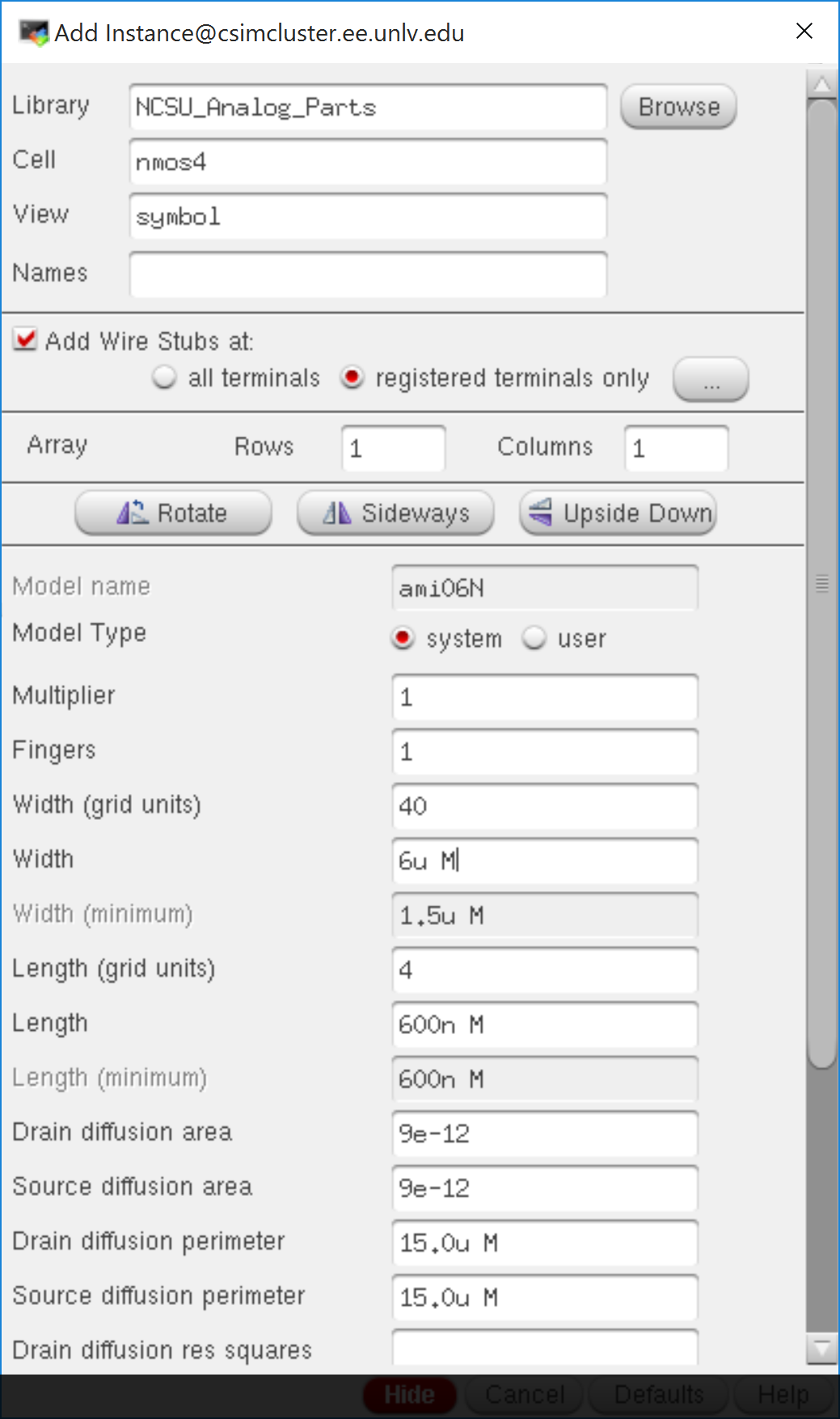
I set the 'Gate' tied to 'VGS' and the 'Drain' tied to 0.
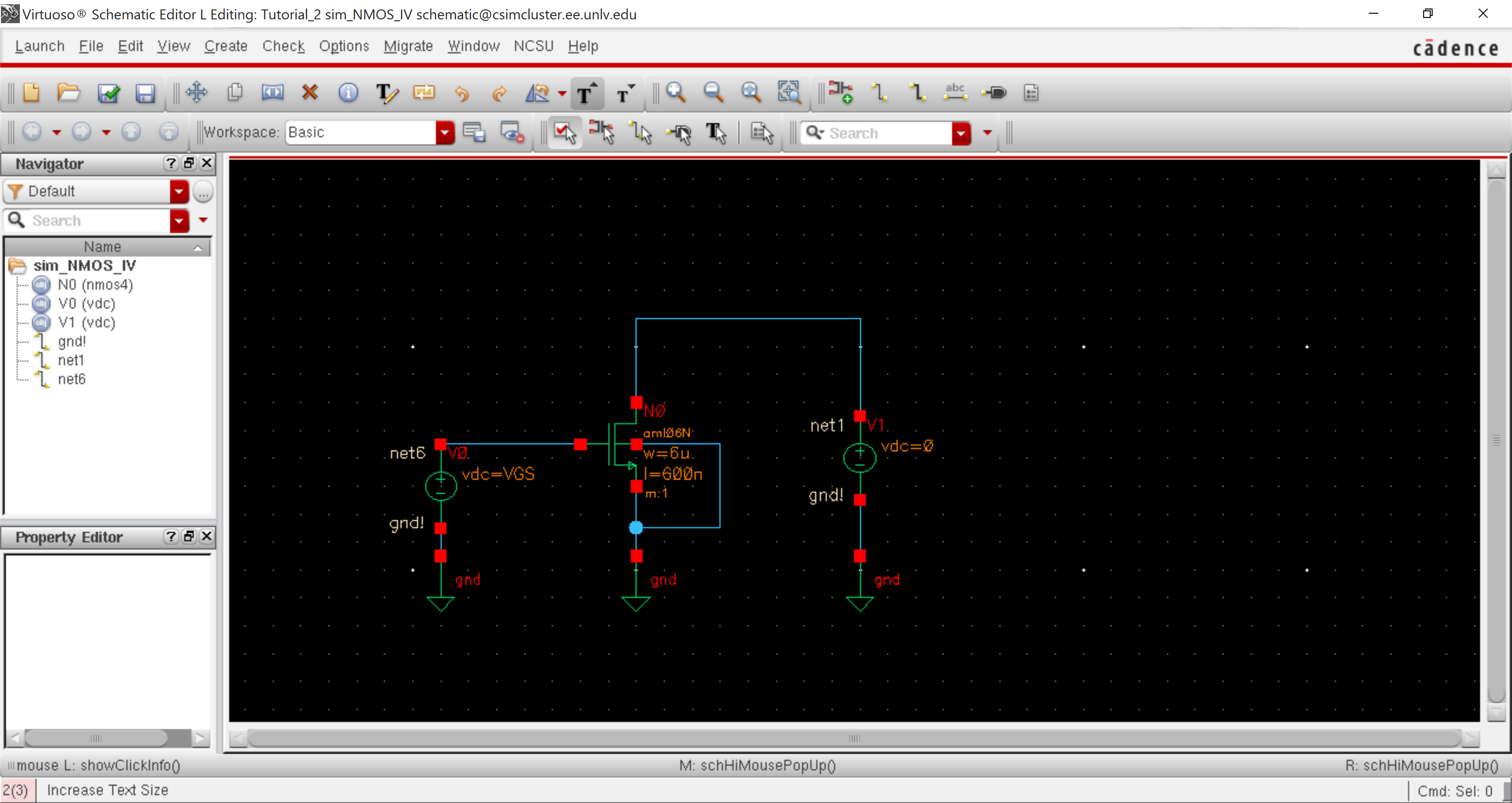
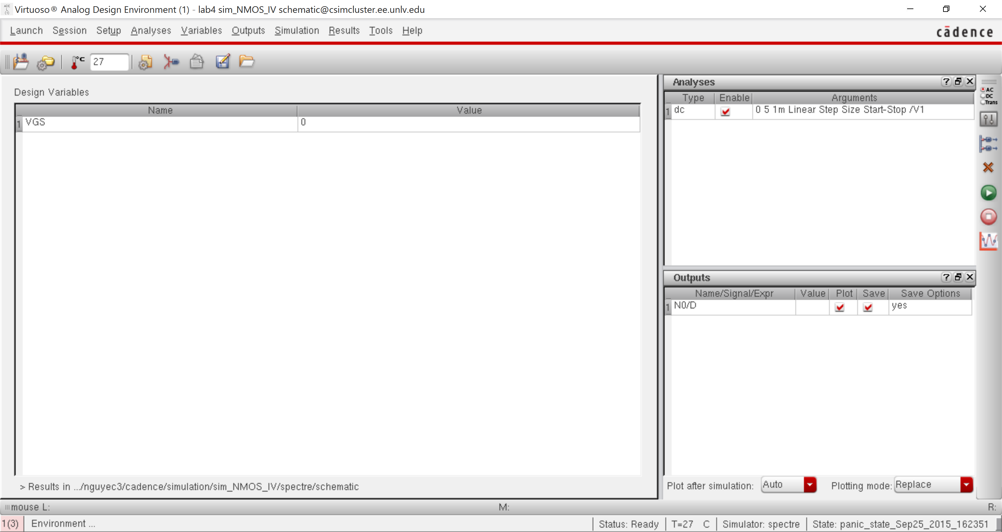
I check and save, and Lauch ADE L to ensure the simulation using the corresponding model.
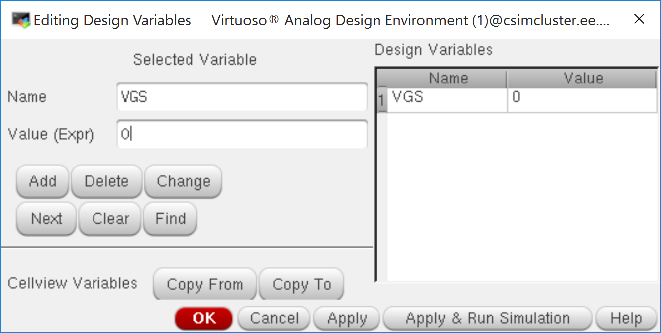
Create "VGS" following Varibles->Edit
I choose Analyses->Choose->dc
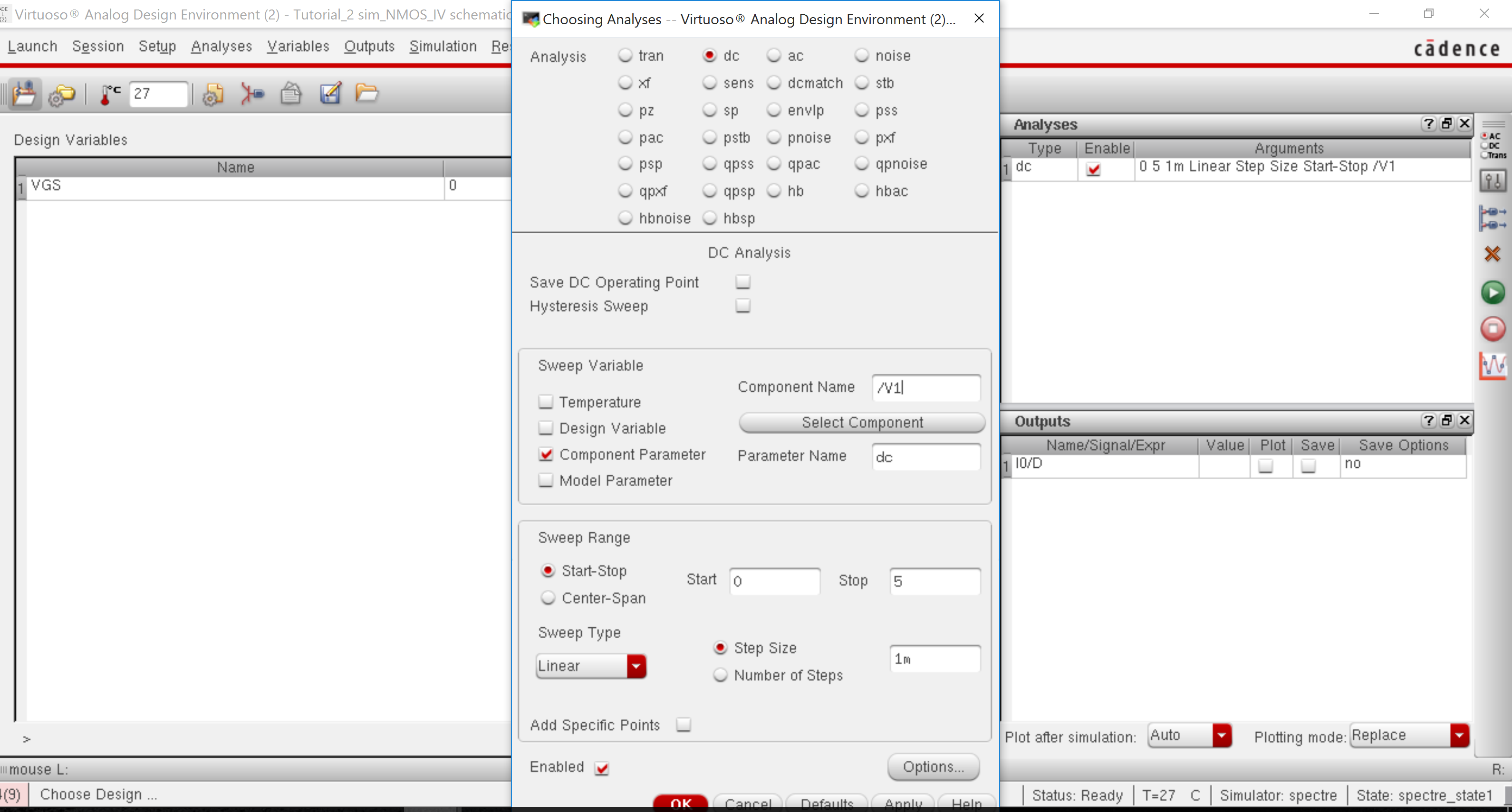
The setting will sweep VDS from 0 to 5V using 1mV step using Tools->Paramrtric Analysis
Next, I select Outputs->To Be Plotted->Select on Schematic
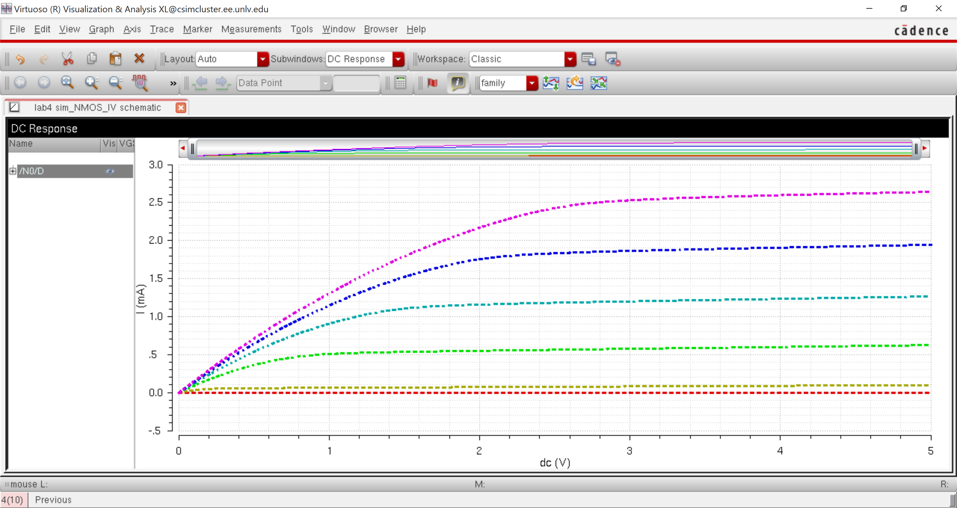
Simulation ID vs VDS (NMOS 6u/600n)
2. ID
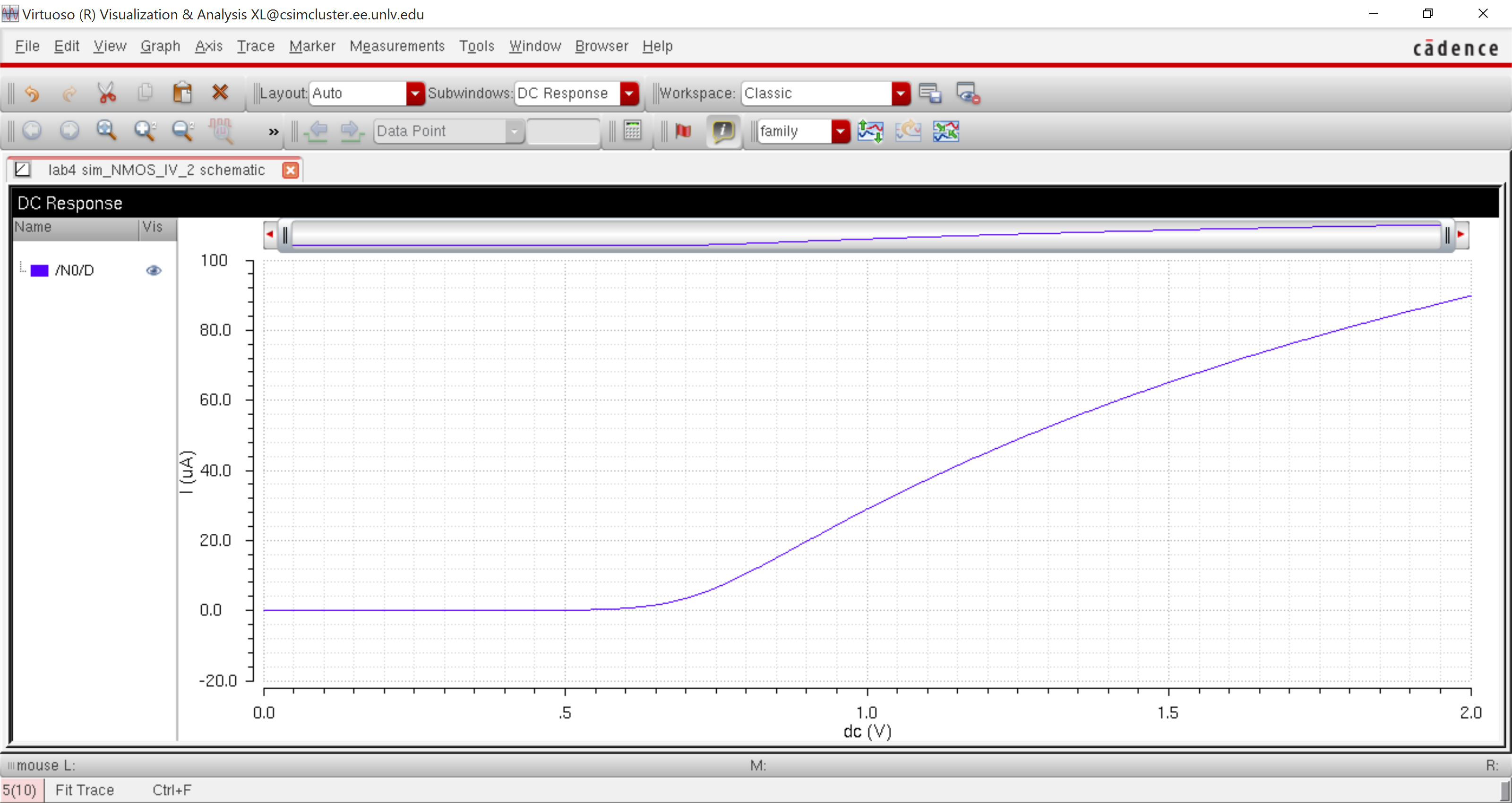
vs. VDS of an NMOS device for VDS = 100mV and VGS varies from 0 to 2V (W/L= 6u/600n)
Lauch ADE and set the following simualation settting using previous steps. VGS will swept from 0 to 2V using 1m linear step
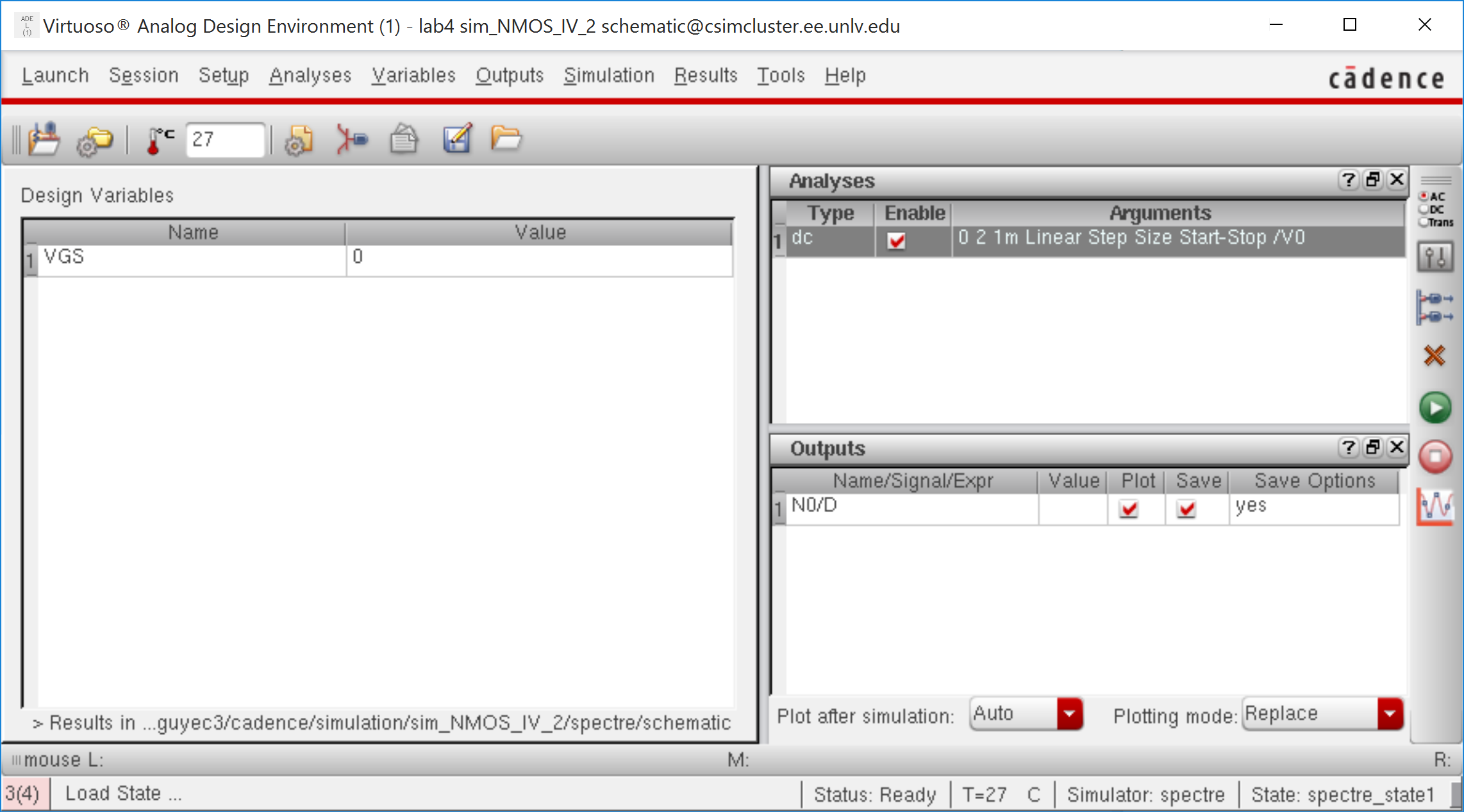
Simulation ID vs VGS (NMOS 6u/600n)
The schematics and simulations of PMOS:
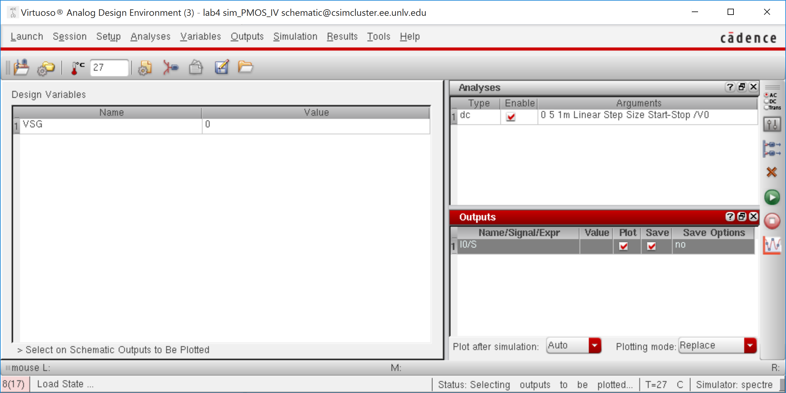
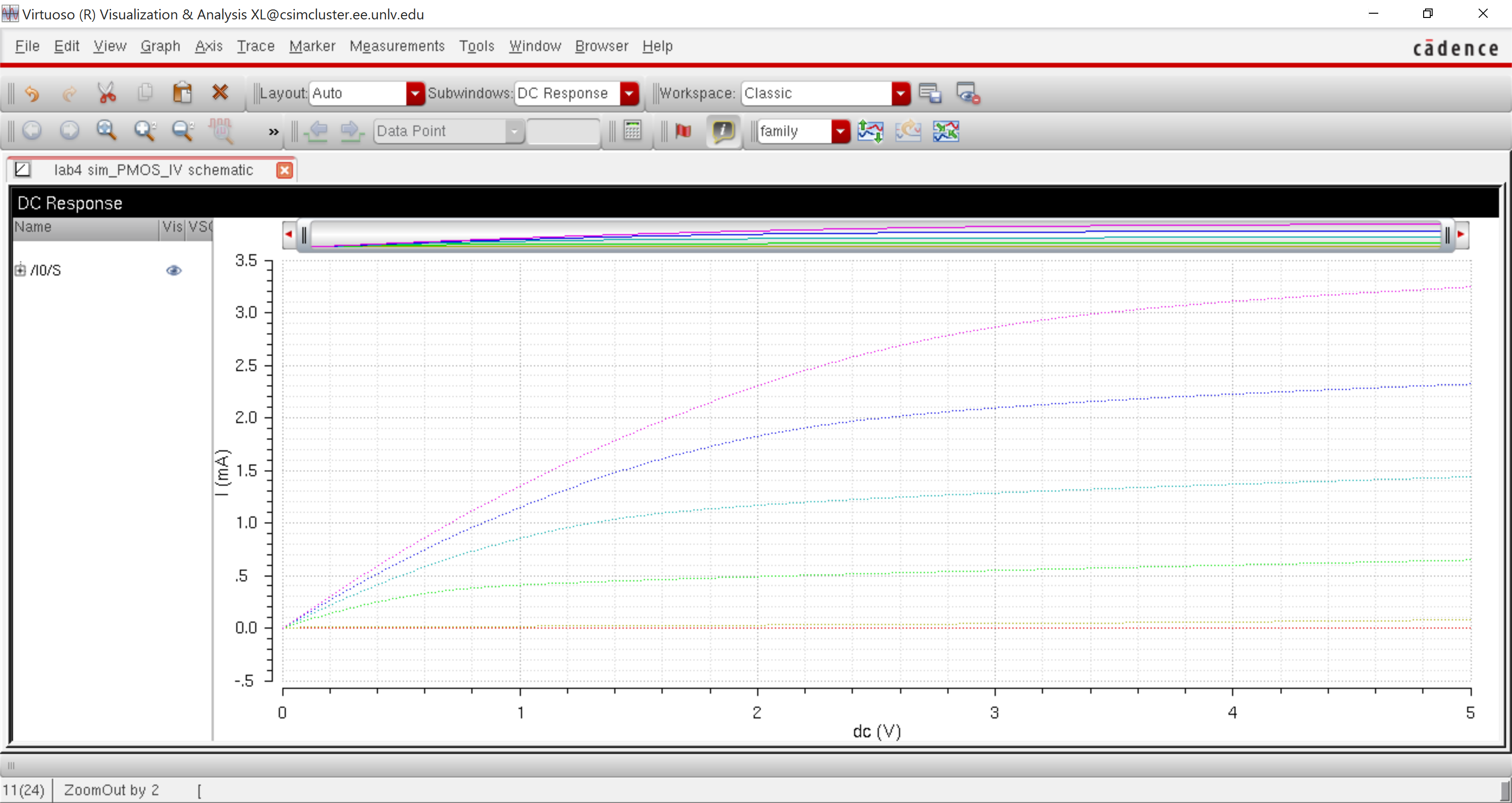
1, ID
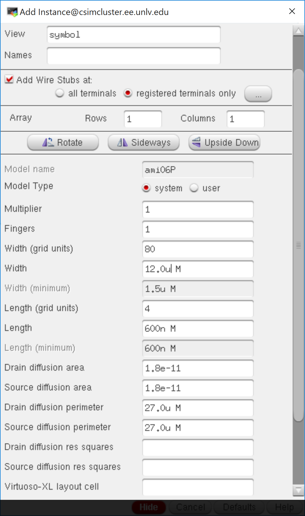
vs. VSD of an PMOS device for VSG varying from 0 to 5 V in 1 V steps
while VSD varies from 0 to 5 V in 1 mV steps (W/L= 12u/600n)
and
I check and save, and Lauch ADE L to ensure the simulation using the corresponding model.
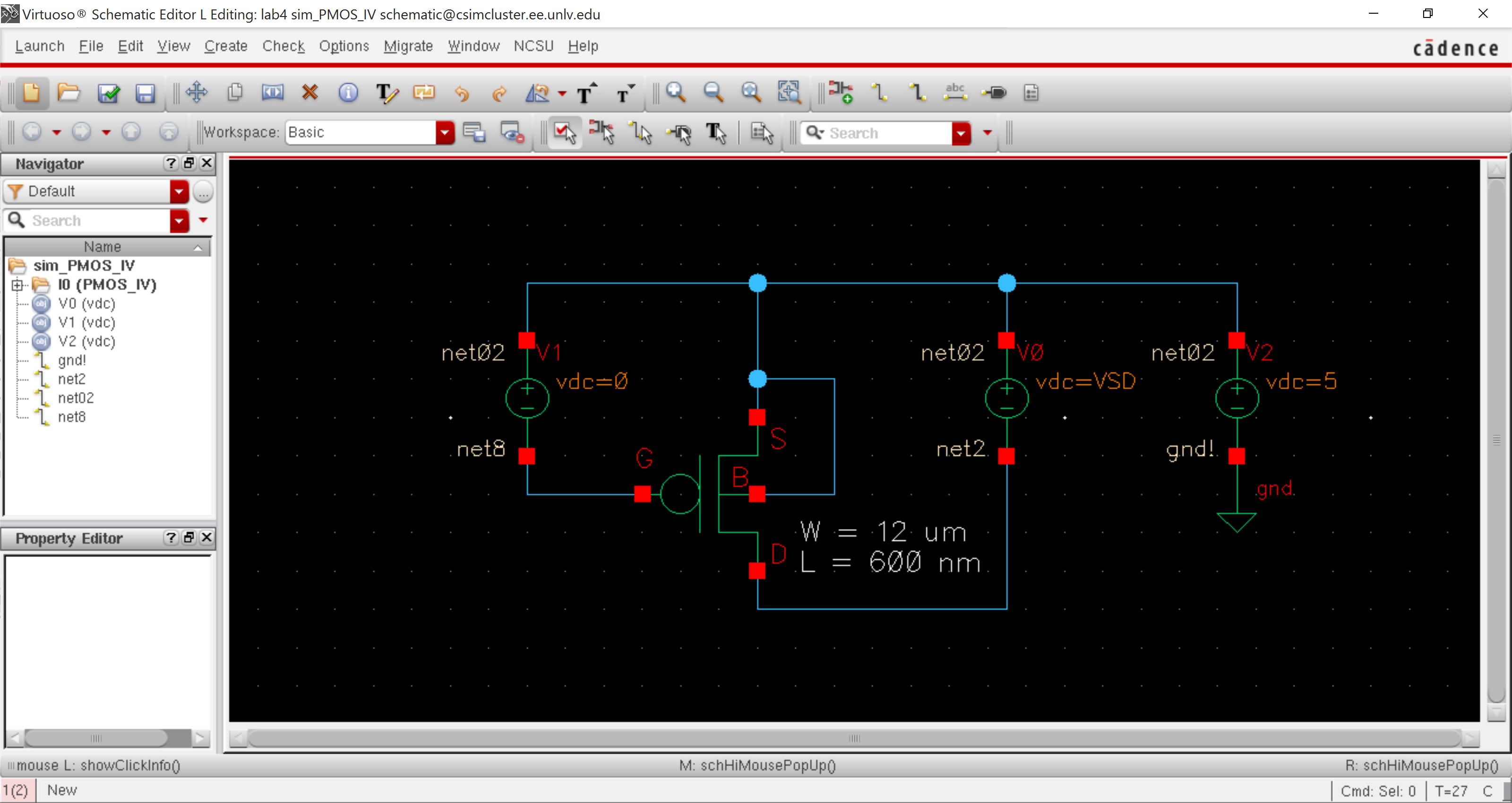
Draft the following schematic
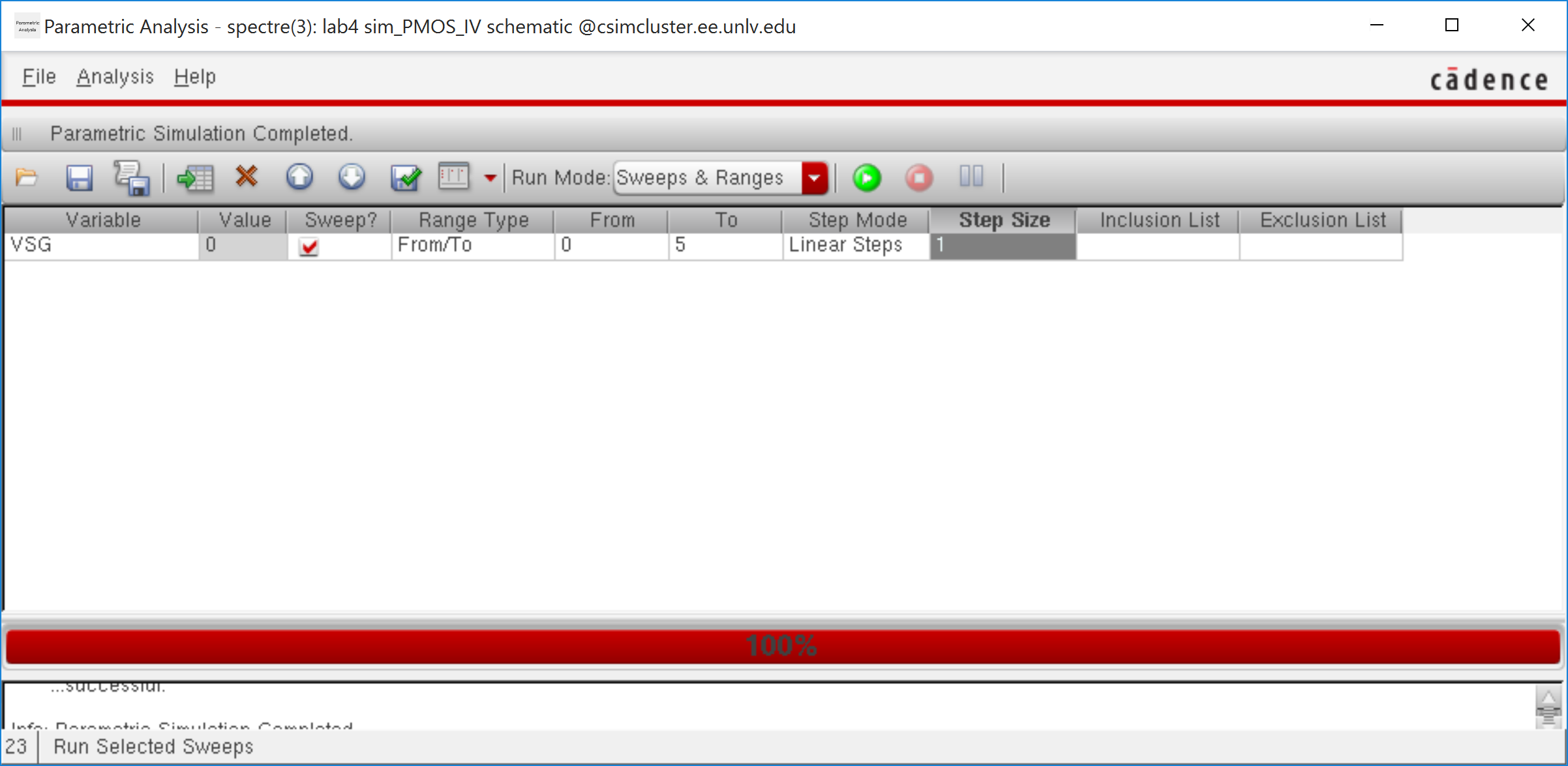
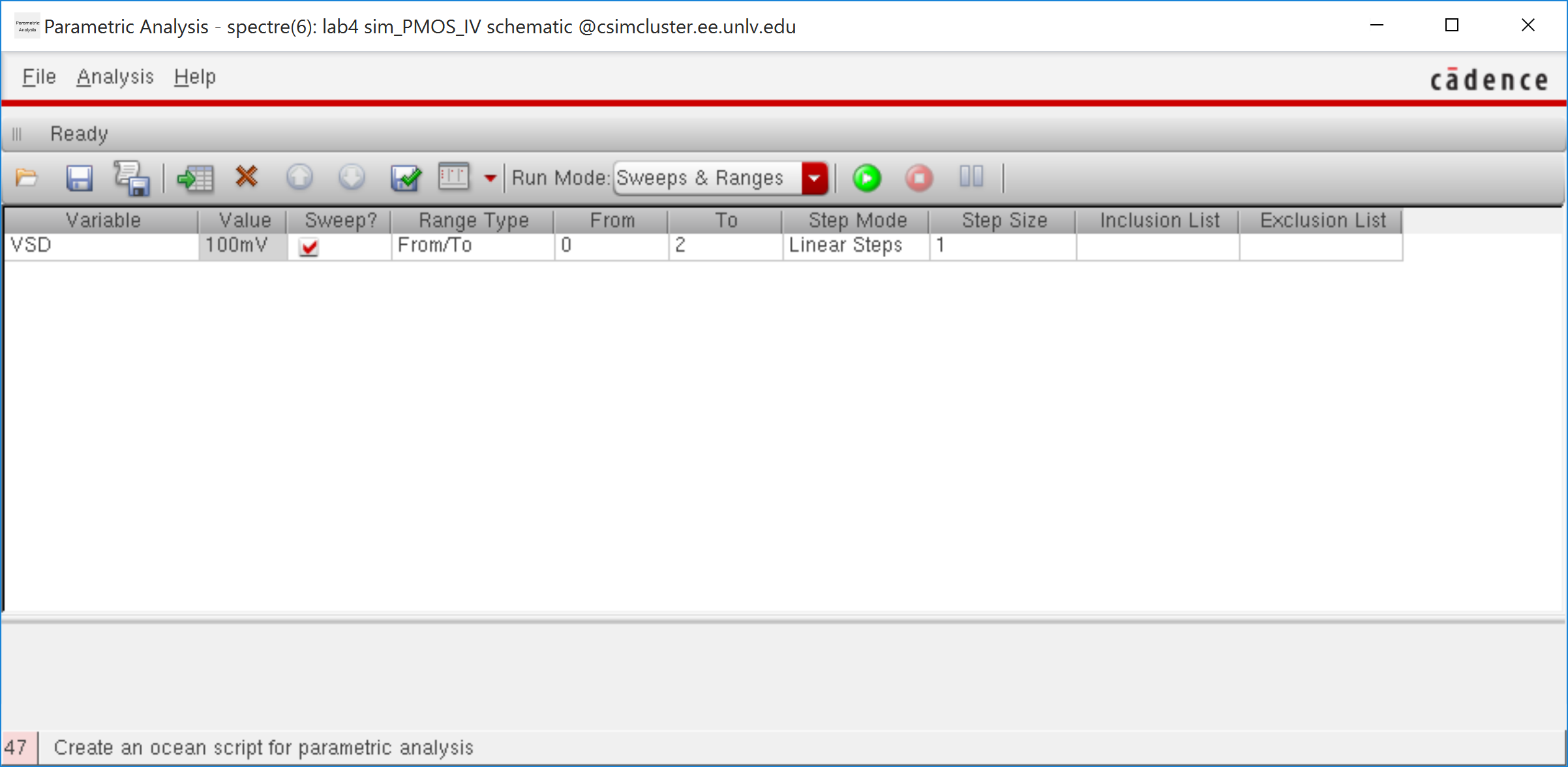
I choose to edit parametric following seen picture below and hit 'play'.
Simulation ID vs VSD (PMOS 12u/600n)
2. ID
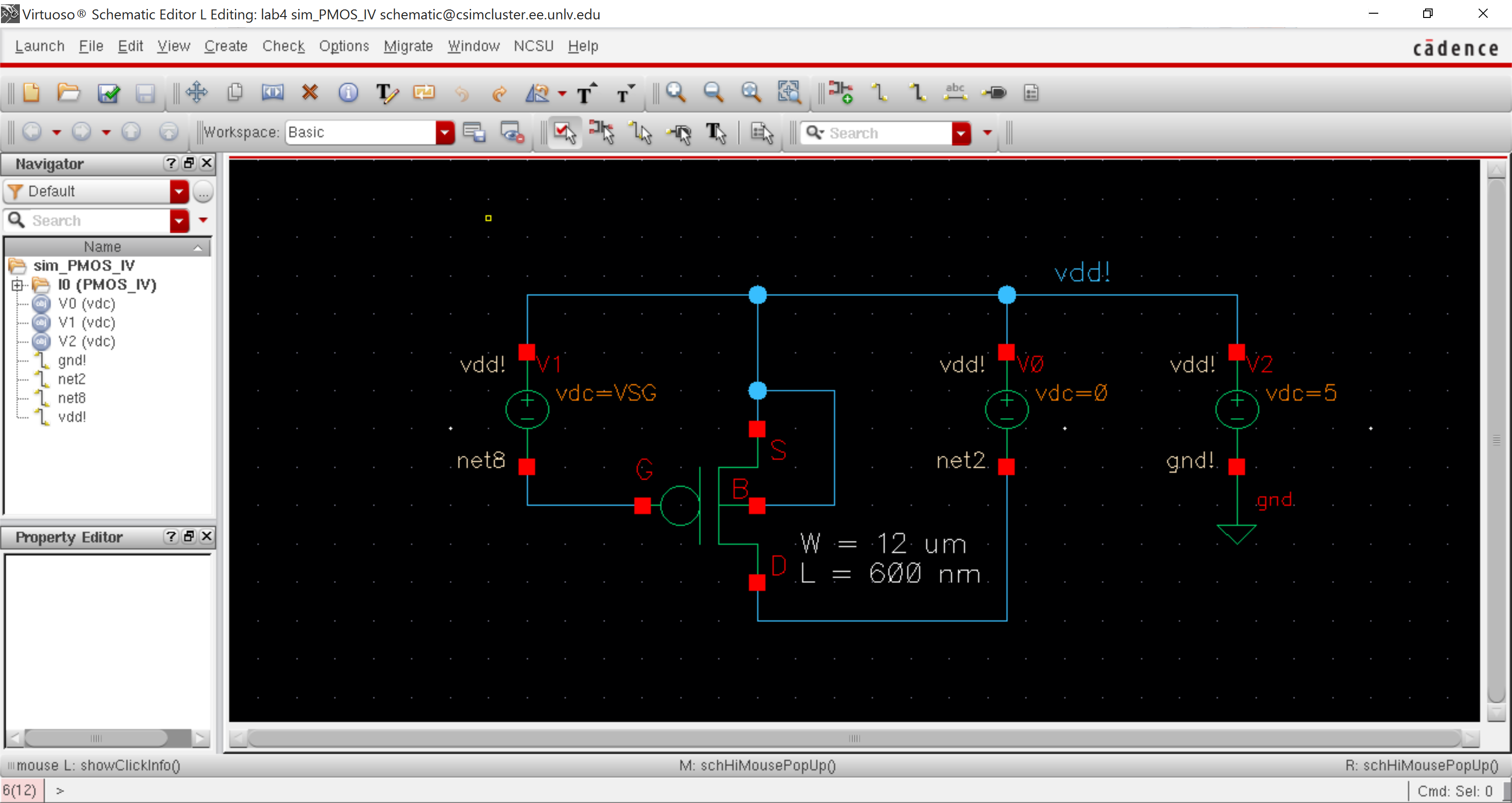
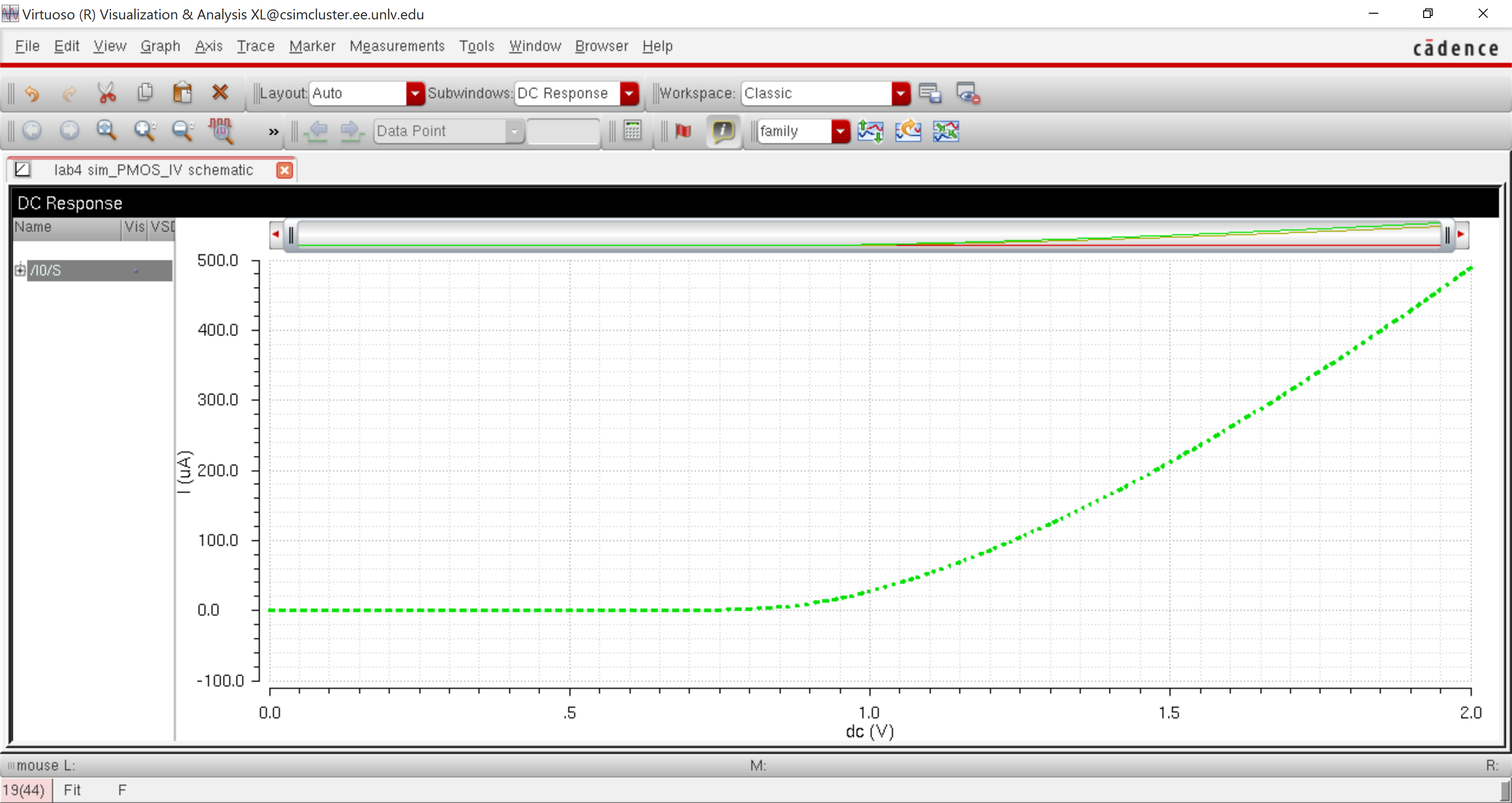
vs. VGS of an PMOS device for VSD = 100mV and VGS varies from 0 to 2V (W/L= 12u/600n)
Draft the follwoing schematic
Lauch ADE setting to set the following
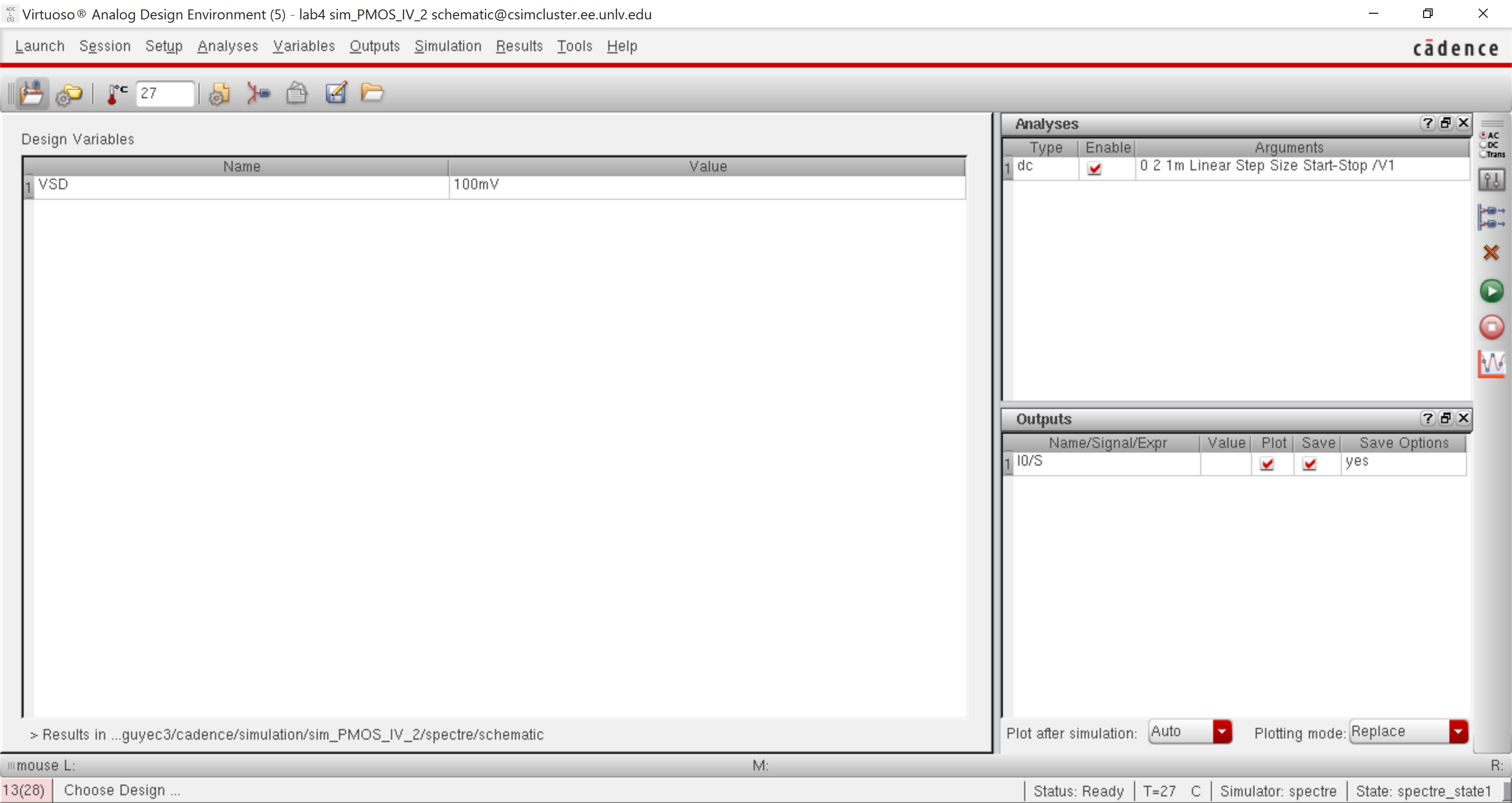
Set VSD is set to 100mV and VSG sweepts from 0 to 2V using 1mV steps and hit 'play'
Simulation ID vs VSG (PMOS 12u/600n)
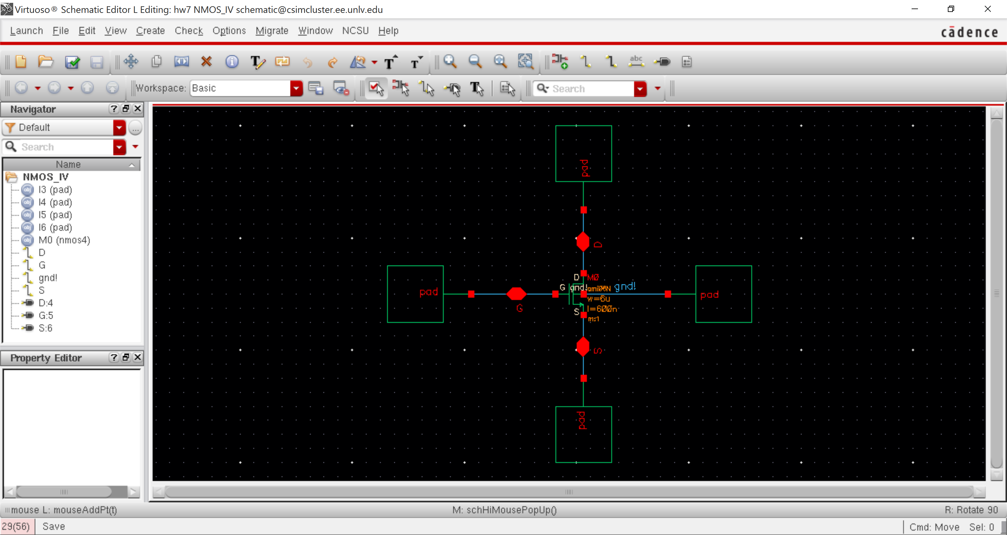
NMOS connected to Probe Pad Schematic and check save
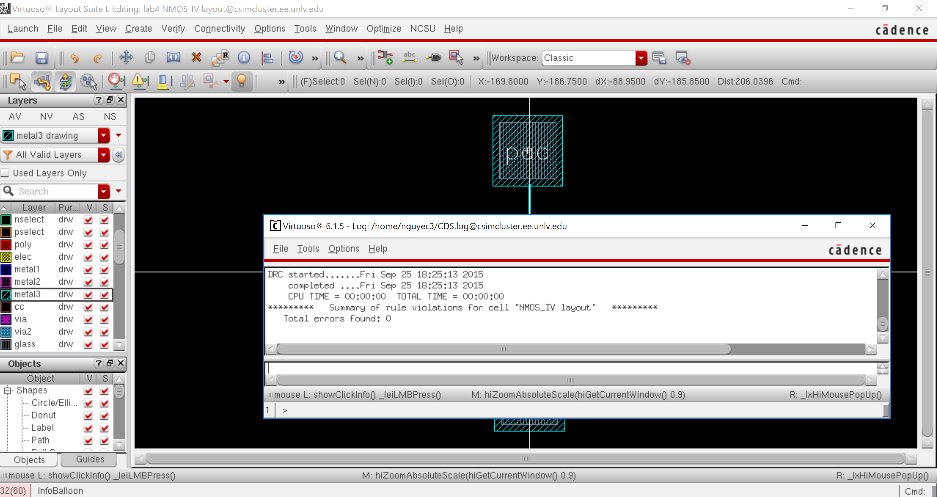
NMOS connected to Probe Pad layout, DRC, LVS, and Output
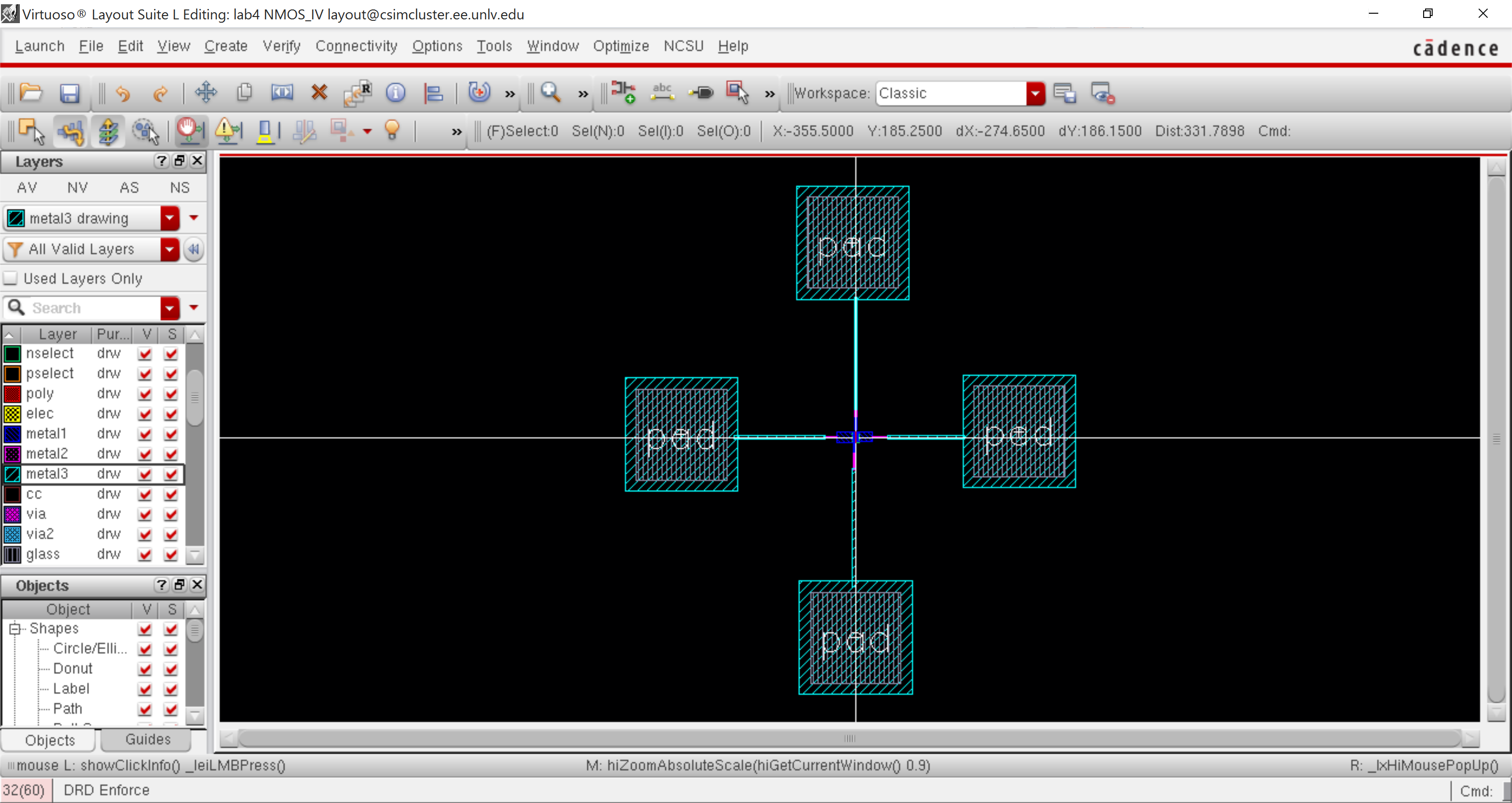
NMOS connected to 4 pads with DRC:
NMOS connected to 4 pads with LVS
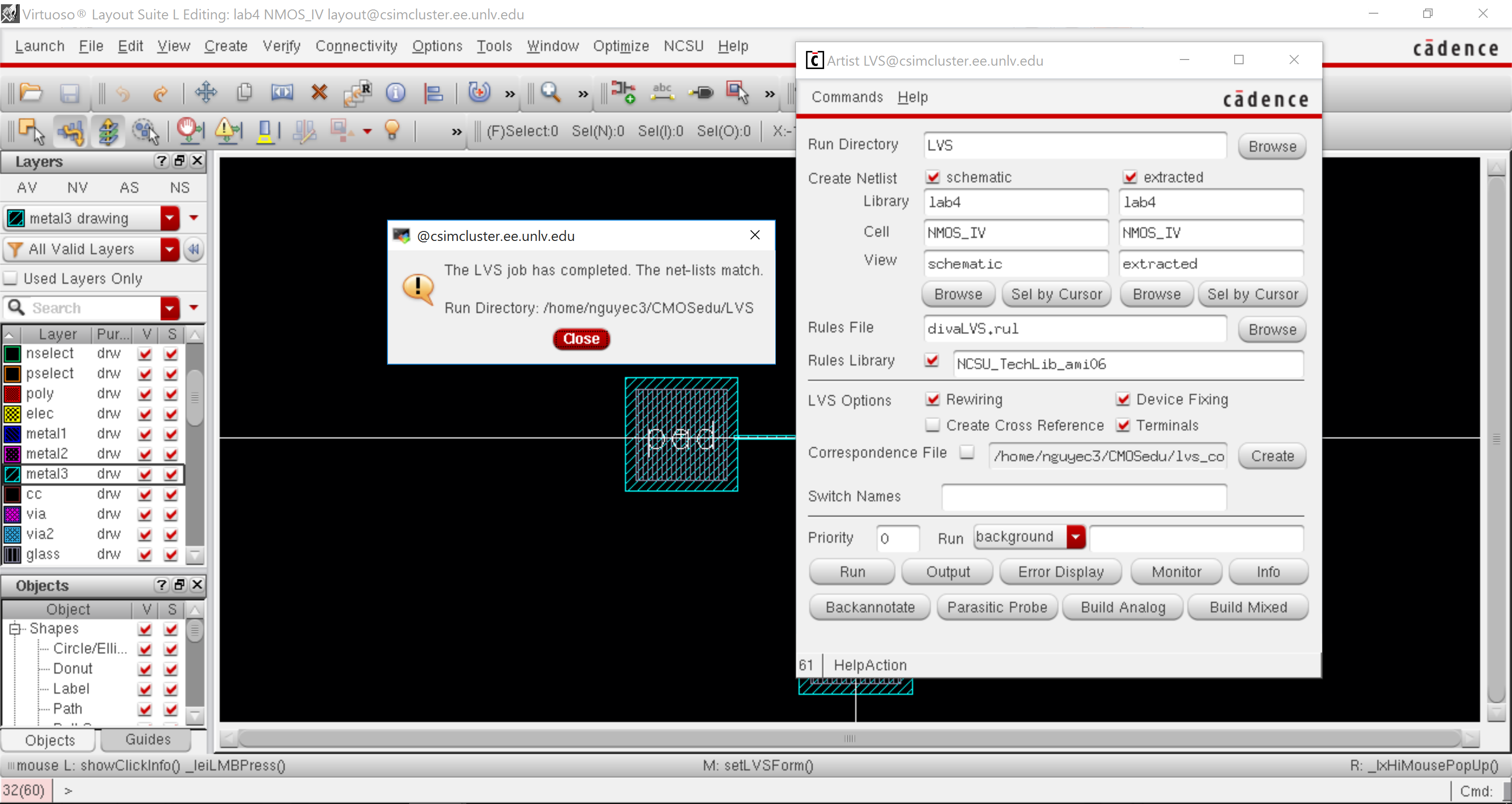
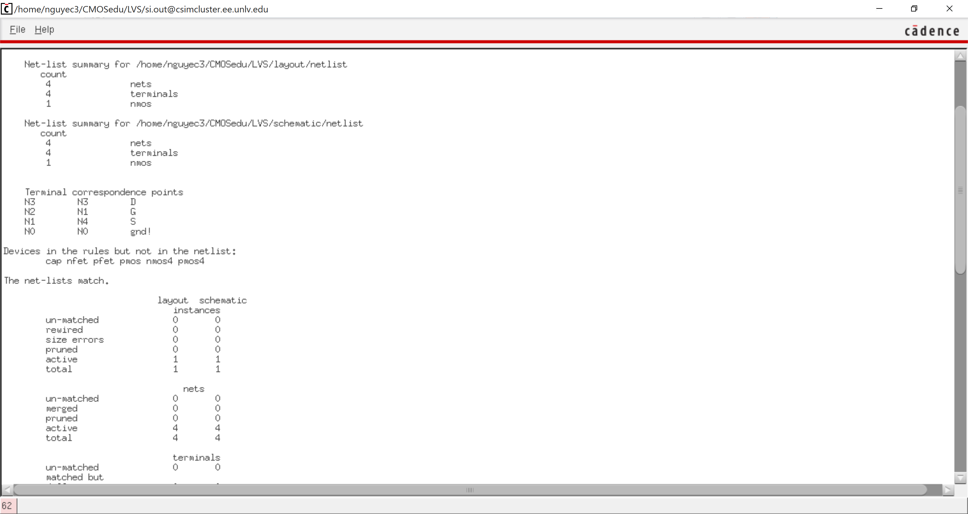
NMOS connected to 4 pads with LVS Output:
PMOS connected to Probe Pad Schematic and check save
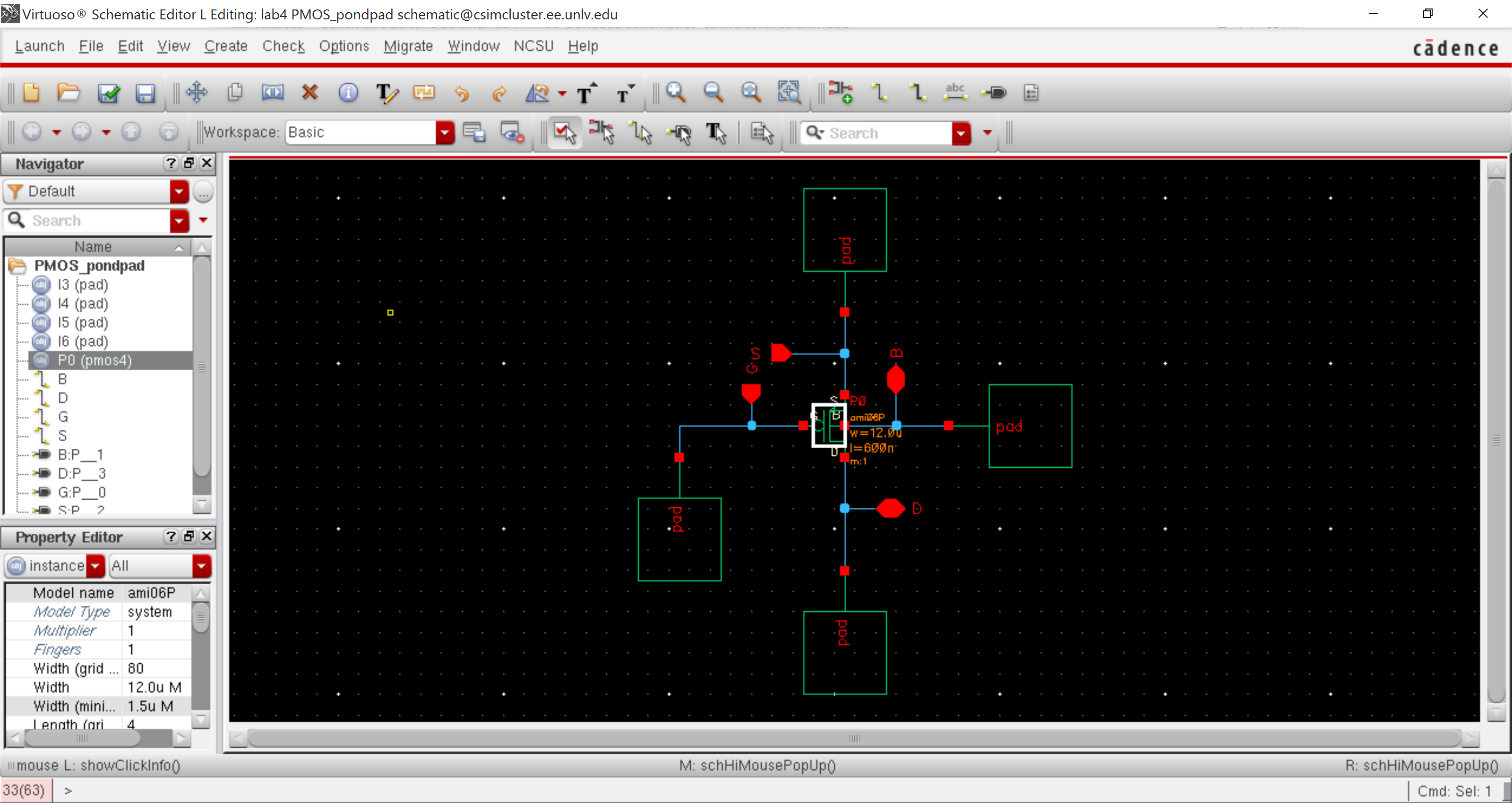
:
PMOS connected to Probe Pad layout, DRC, LVS, and Output
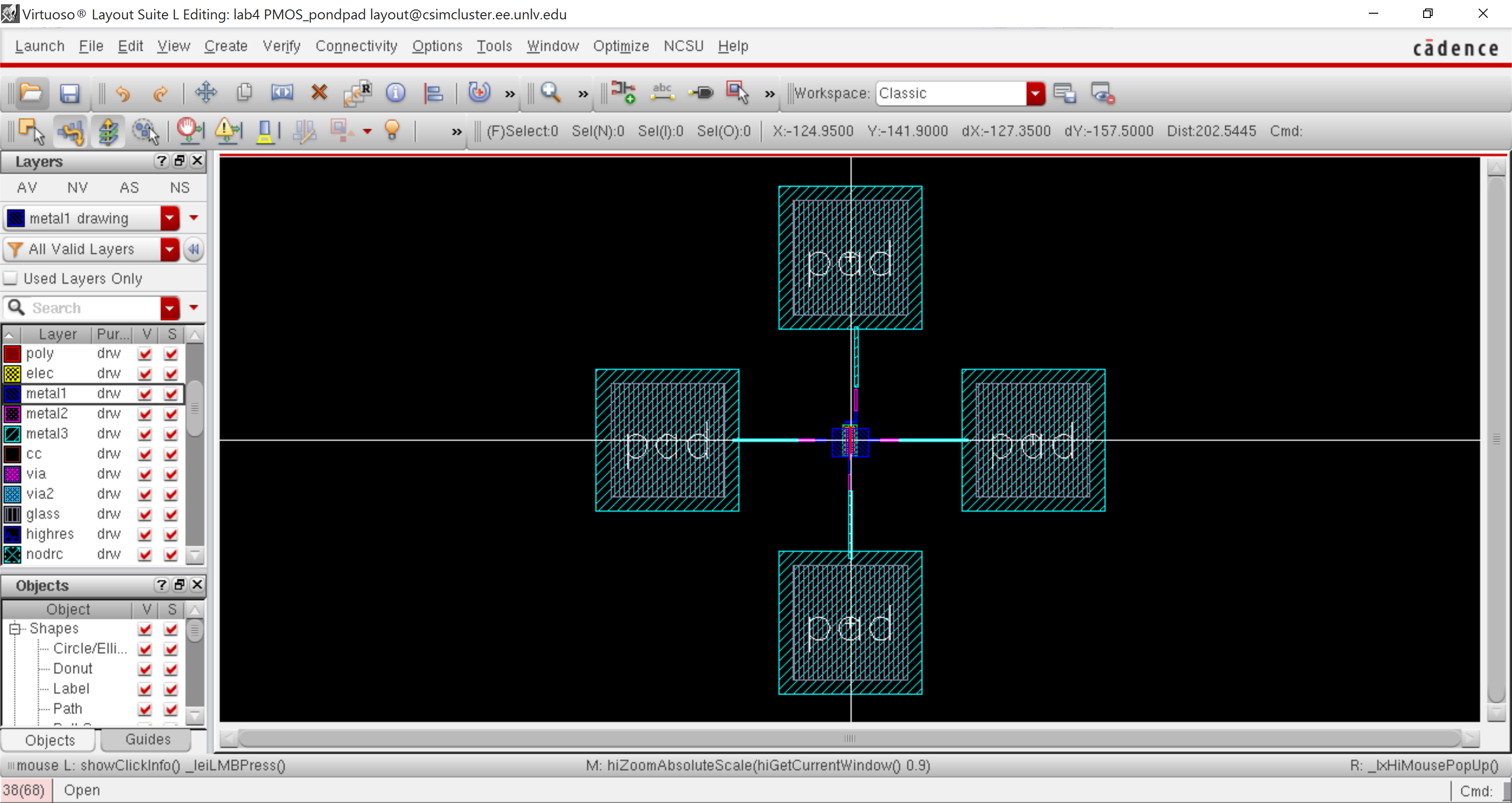
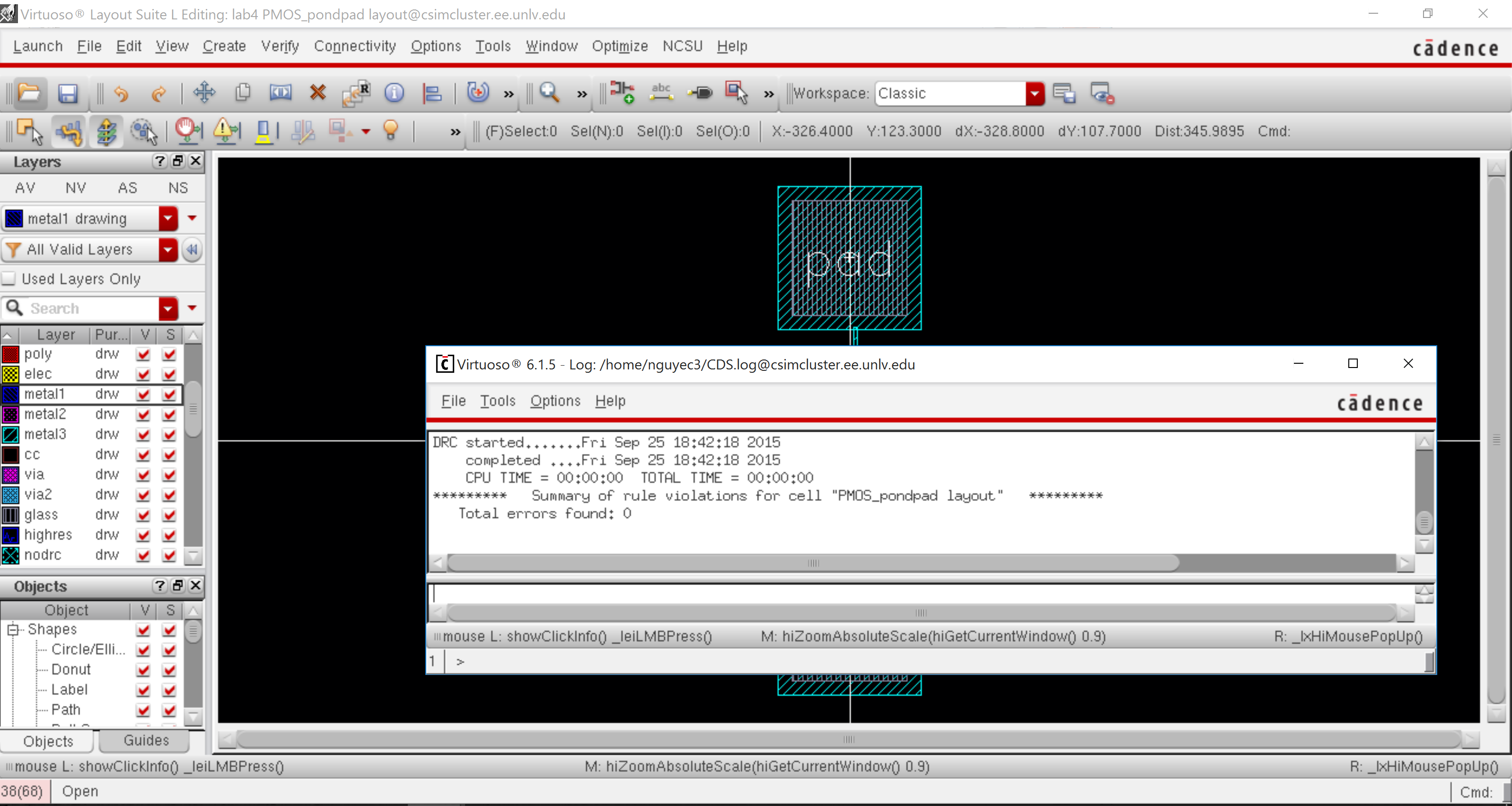
PMOS connected to 4 pads with DRC:
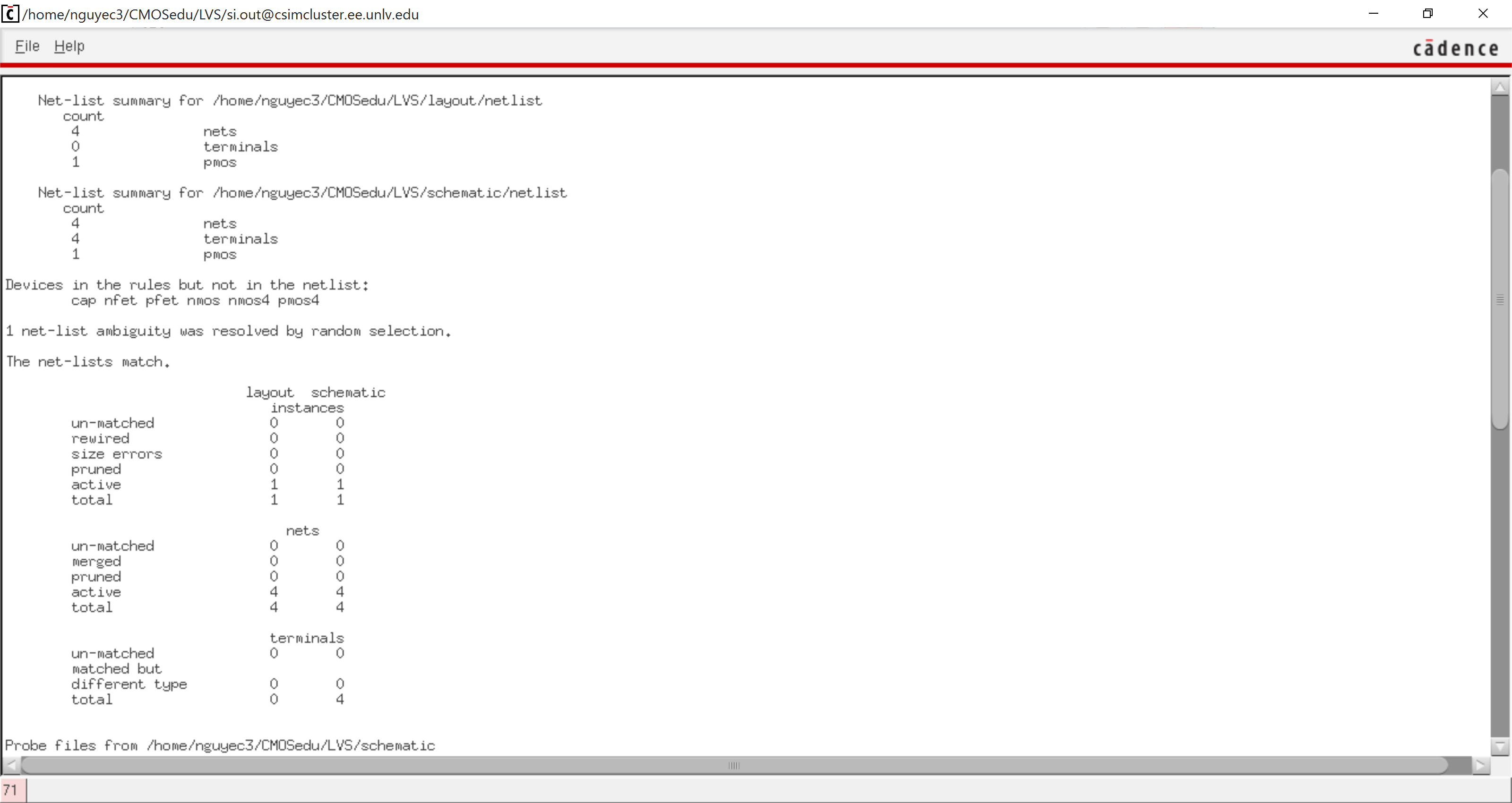
PMOS connected to 4 pads with LVS
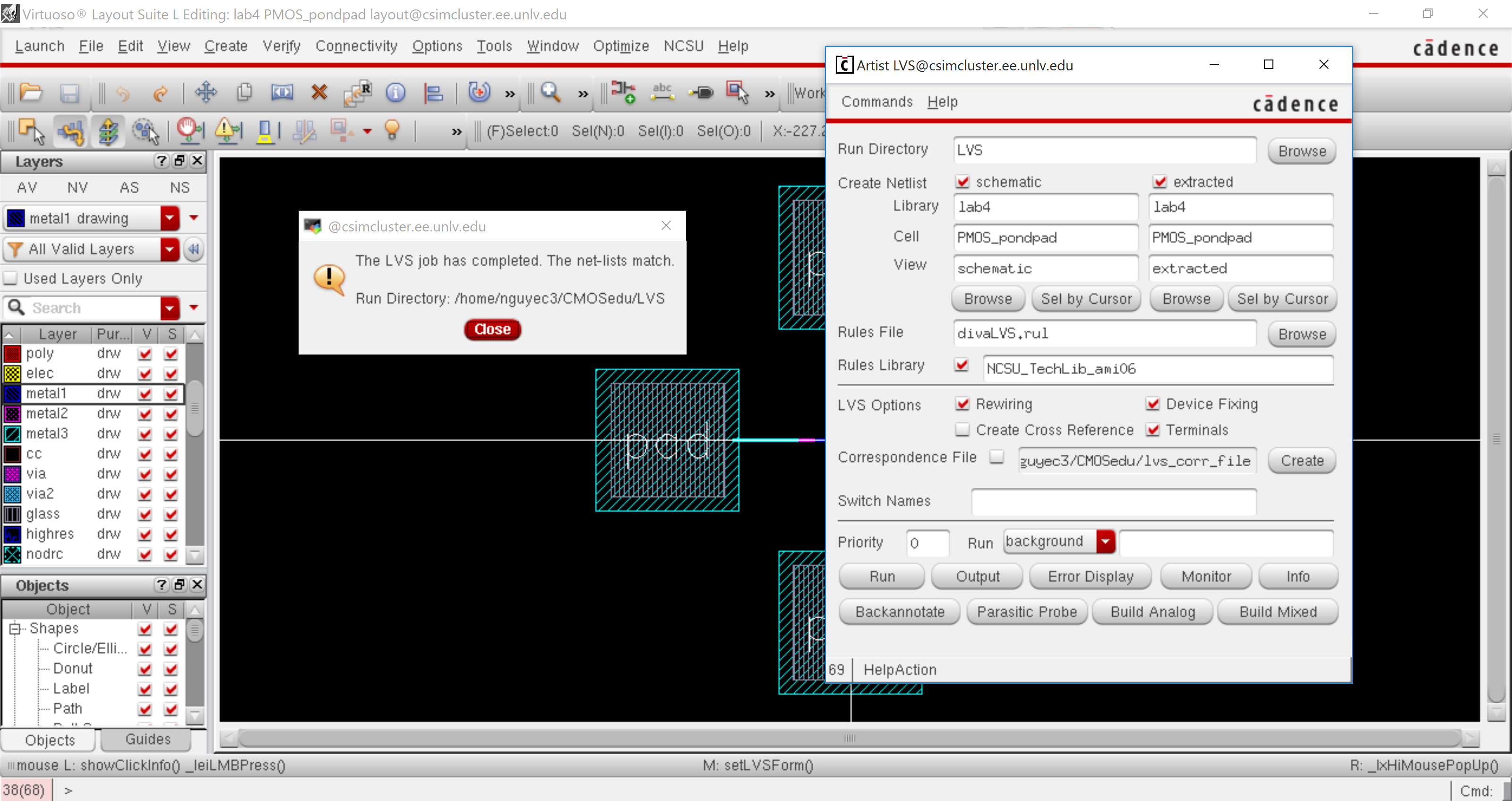
PMOS connected to 4 pads with LVS Output:
Saving my works into dropbox and email:
and

Return EE 421L Labs


