EE421L, Lab5
Mari Gilligan
Email: mgill19@unlv.nevada.edu
9-28-15
Prelab:Going through the tutorial 3-Design-Layout and simulation of a CMOS inverter
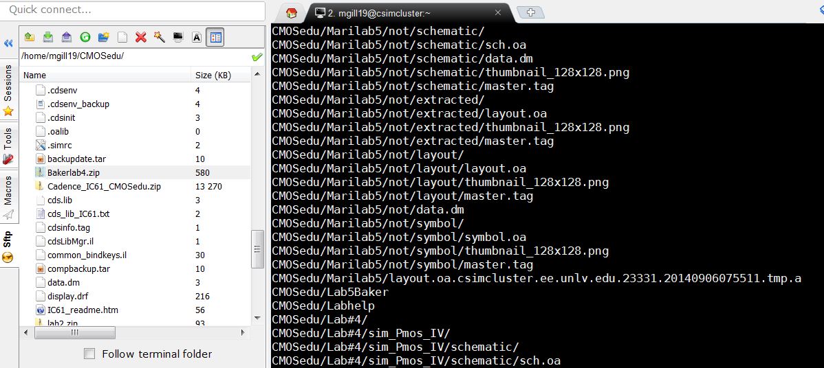
Bch up my project ar ususal through moaXterm and then ,
starting
with going to Mab-X-term and launch virtuoso,and then we will going to
copy library-2 to a new library that we need to creat and call it
Tutorial-3.
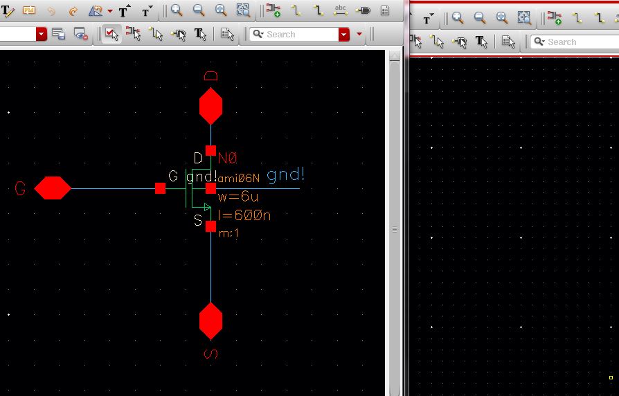
Next we will creat a new cell viw schematic ,and after
the window pops-up we will open the NMOS-IV schematic as well, like
what you can see here.
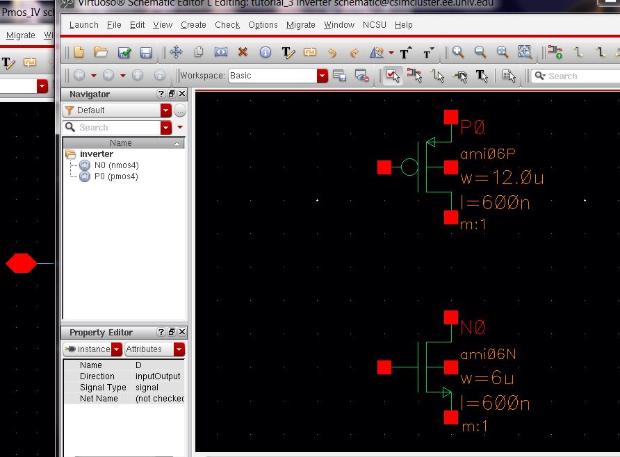
we
are going to copy the NMOS symbol from the NMOs IV cell into the
inverter cell,make sure the two windows are open ,then press copy(C)or
use the menu and then click on the nmos 4symbol and drag over into the
inverter window .
after you are done close the NMOS_IV window and open the PMOS-IV window.do the same thing for PMOS4 to get this :
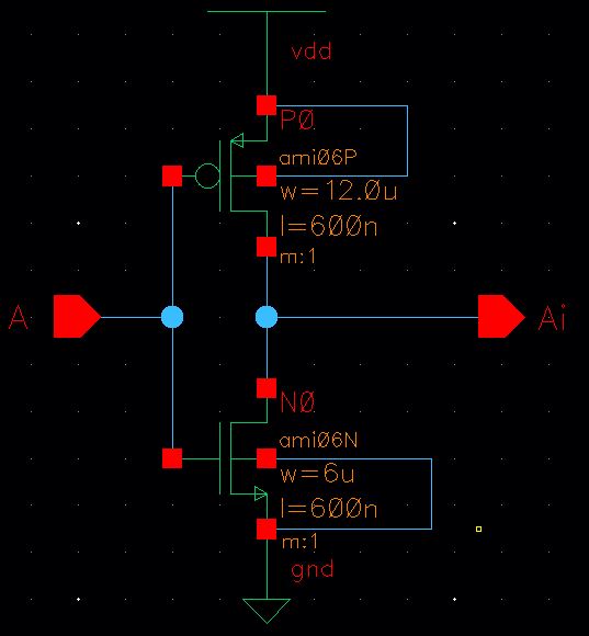
press
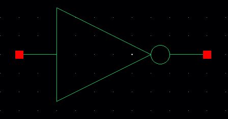
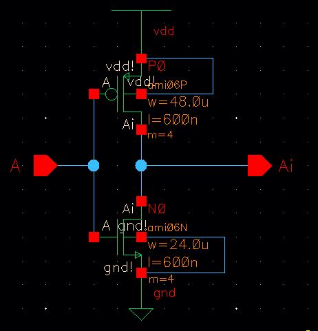
instantiate or (i) to get vdd and gnd supply nets.and place them in the
schematic,wire up the inverter and add pins as you can see here.the
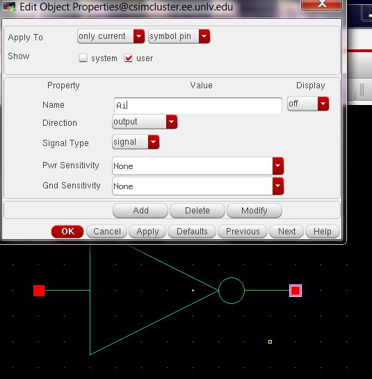
Apin is input direction and Pin Ai is an output direction.
Like what i have here.
.
check and save.
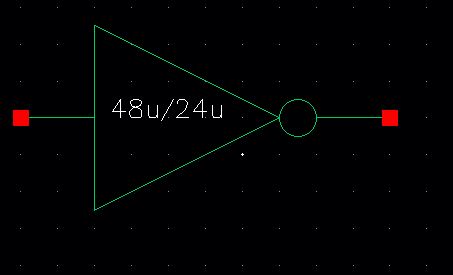
next use the menu item to creat ->cell view ->from the cell view to creat the symbol for the inverter.
delete everything in the inverter's symbol view except for the pins.draw the inverter symbol (creat->shape->line/circle).
make sure the pin names are correct since we are not using them here
but you can still check if they are correct by selecting all of thenm
and verifying that they are in the right location(A as an input ,Ai is
the inverter's output)
check and save the inverter symbol ,and Next:
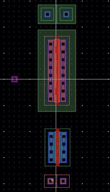
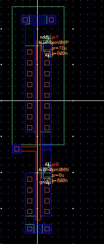
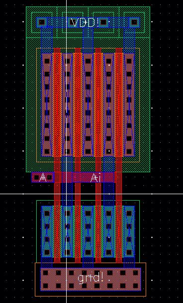
creat
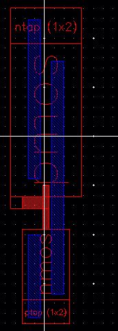
the layout view for the inverter ,Add the following cells
(nmos,pmos,ntap,Ptap,and m1-Poly)to the layout view as seen below ,you
can instantiate these cells as you we already know how,press i.
make sure nmos is 6u/0.6u and pmos is 12u/0.6u and the ntap and ptap use two colums.
.
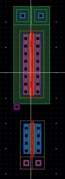
Next
align the cellls until you get something similar to what is seen
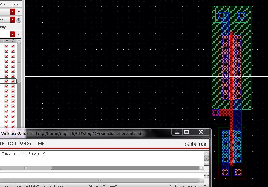
here,DRC your layout to ensure no errors,fix if so ,save the layout.
.
Add rectangles on the poly and metal1 as seen below.
DRC and save your design .
.
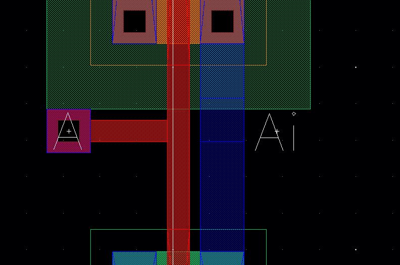
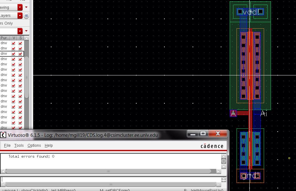
Next add pins on metal1 for gnd!,Vdd!(both have a direction of inputoutput),A (input),and Ai(output).
DRC and save the design
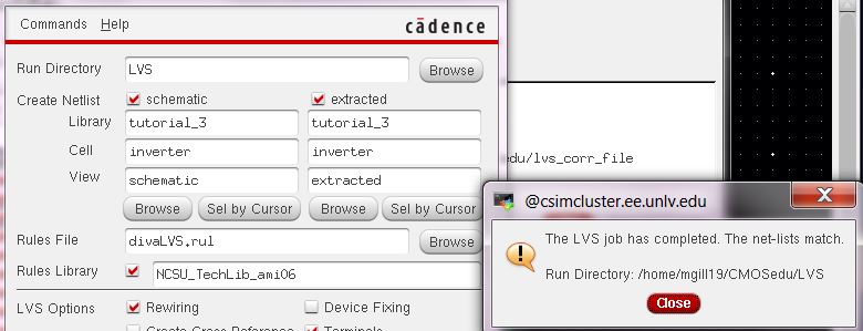
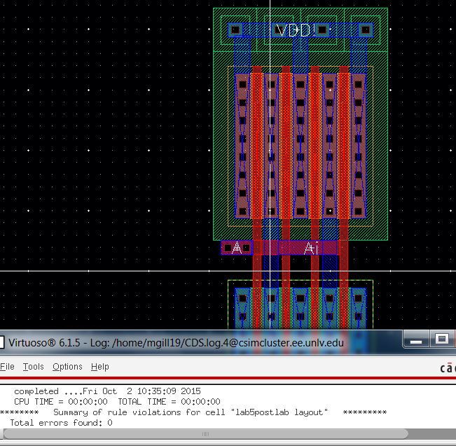
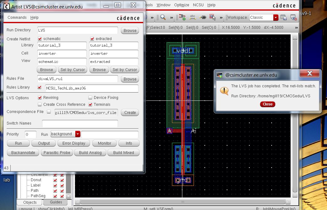
Next run extraction on the layout:
and try to do the LVS on the inverter:
,now we are reday to simulate the operation of the ineverter
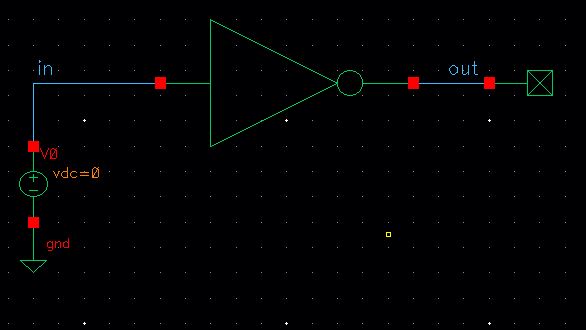
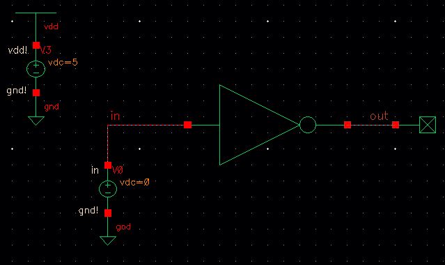
Creat a cell called sim -inverter-dc(file->new->cell view)
draft
the following schemtaic.the symbol on the right is the no connection
symbol (in the basic library ,Misc->noConn)we add this symbol to be
different and to avoid the warnings related to floating pins/nets that
we ignore via the menu item check ->find Marker->ignore,ignore
start
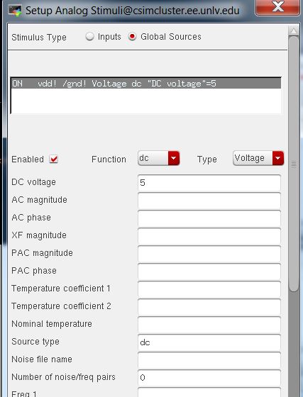
the ADE and selct the model files (setup->model libraries located in
/Home/ncsu-cdk-1.6.0 beta /models/spectre/standalone)
Next slect the analysis ->choose
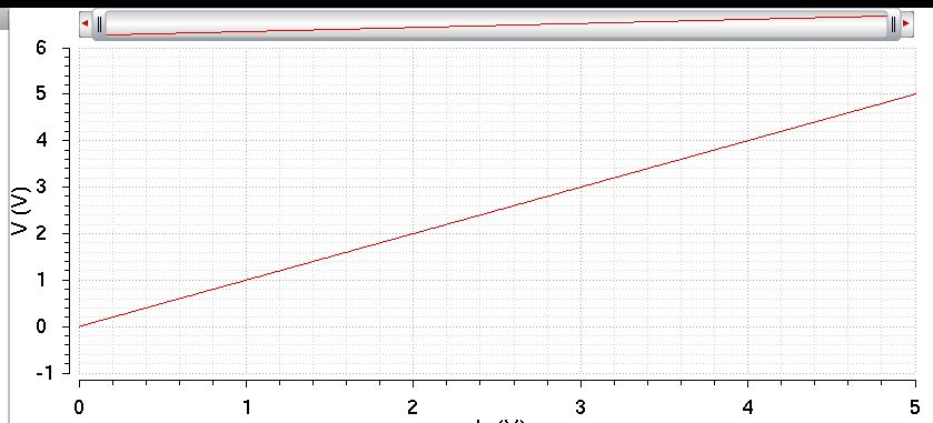
and note that the input vds is named V0.
then go to output ->to be plotted->select on schematic (select in and out)
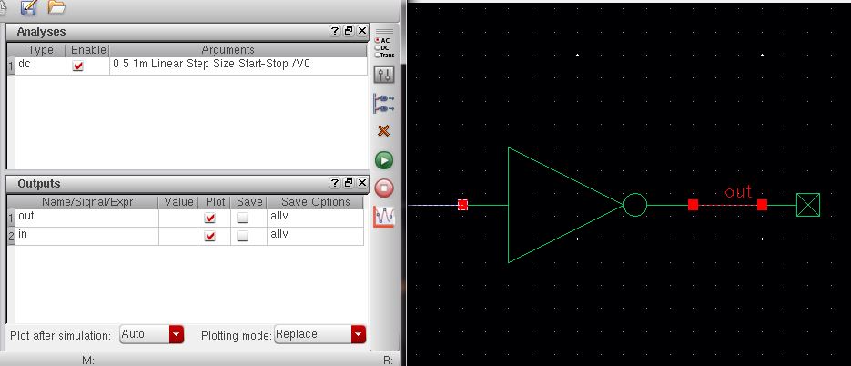
save the state in cell view
neltilst and run the simulation (hit the green button)
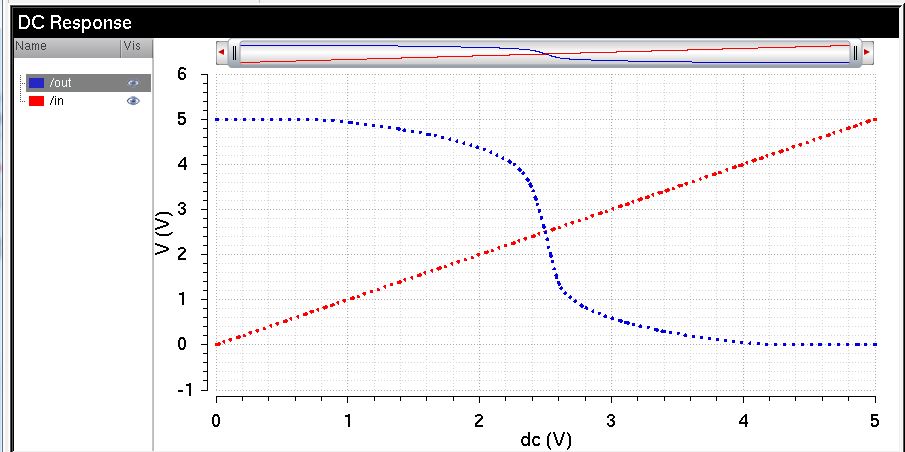
and we get this:
Lets add vdd since we sae that Vout was 0in the simulation.
save
the state (cellview) so we dont have to do this again next time we run
the simulation.hit ok and run the simulation,you should expect to
have this:
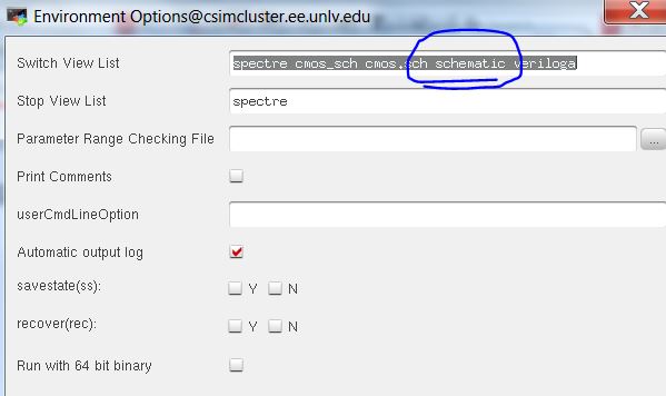
Lets
go ahead and simulate the extracted view at this
piont(setup->Environment and add extracted in fron of schematic like
we did in tutorial-2.
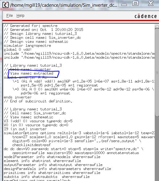
which
gives the same resulit but to make sure that we are simulating the
extracted view and not the schemtaic view go to simulation
->netlist->display:
and make sure you have this:
End of prelab
now
we have to reapeat the process for a 48u/24u inverter,.copy the last
invereter schematic into anew one,pressq and edit the mosfets,W of a
PMOS=48and the W of the NMOS=24. change the multiplier to 4.
copy the symbol that we created for the privous inverter and edit that.
now
we are creating the layout,then open it and go to properties of each
mosfet and change the multipliers .and finish your layout like this and
then DRC it.
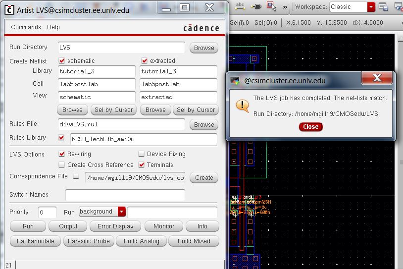
we need to extract and LVS our layout.
now the LVs of the 12u/6u.
we
need to run the simulation of the inverter driving capacitors with a
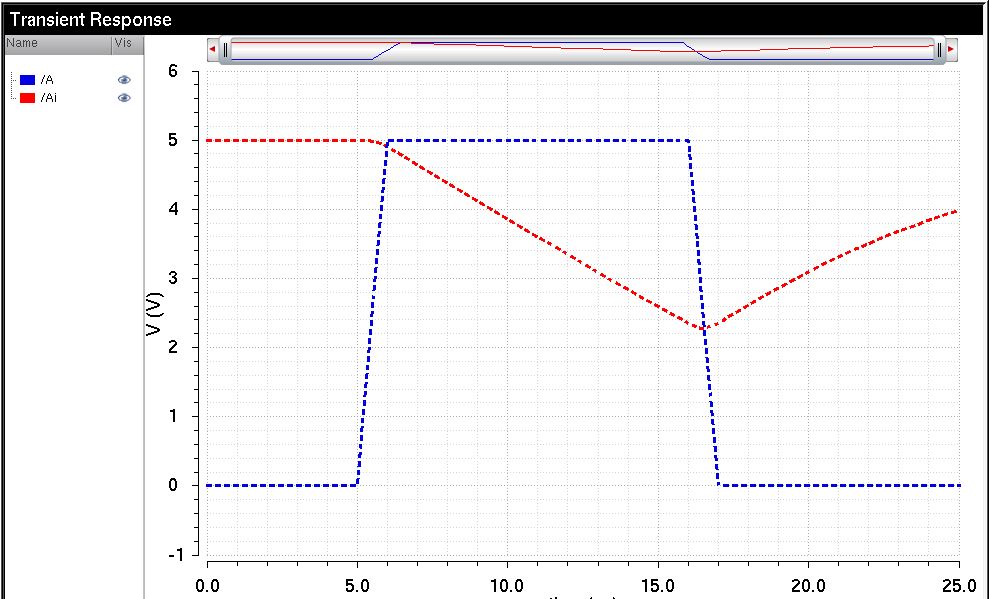
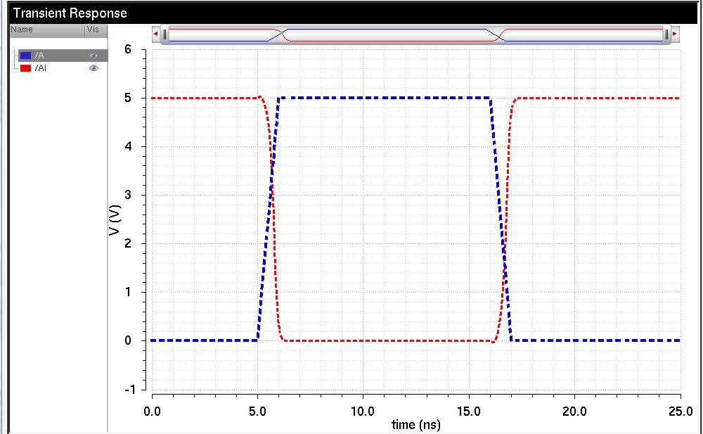
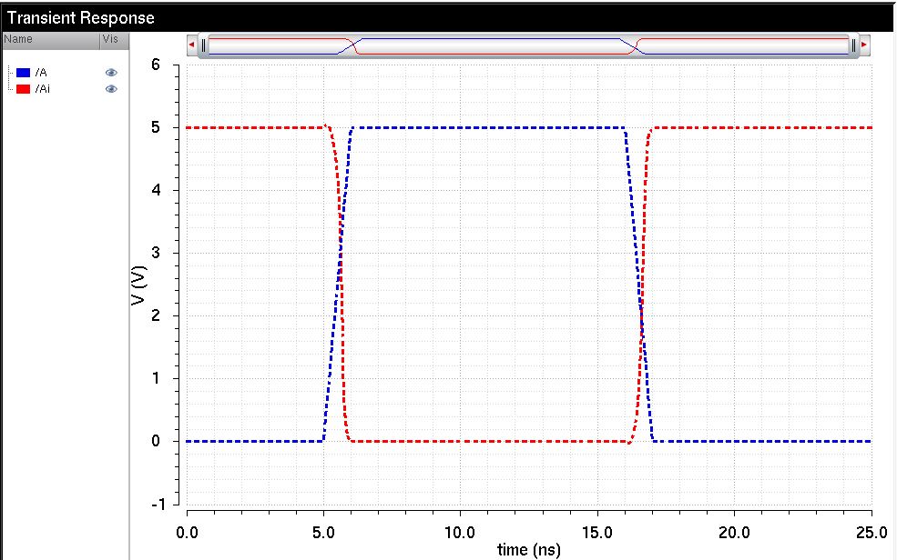
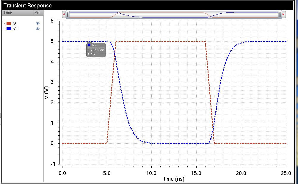
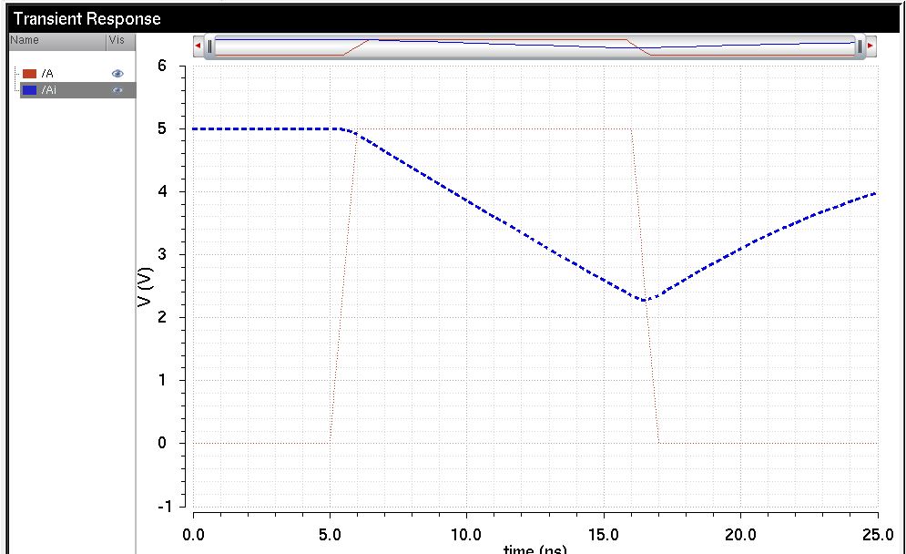
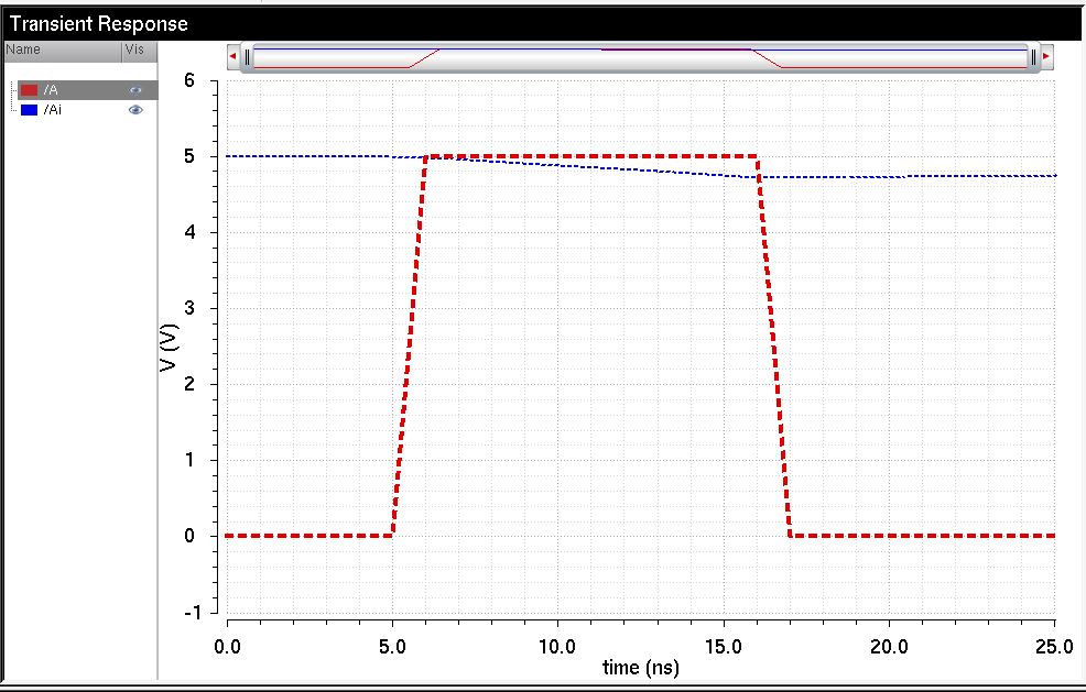
pulse input, we start woth 100 fF load for 12u/6u inverter.and check and save your work.
we change the capacitor values each time and we drive our simulation:
this is my schematic of one example:
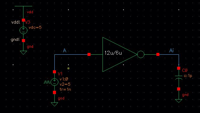
the 100fF Laod .
12u/6u inventer:
48u/24u
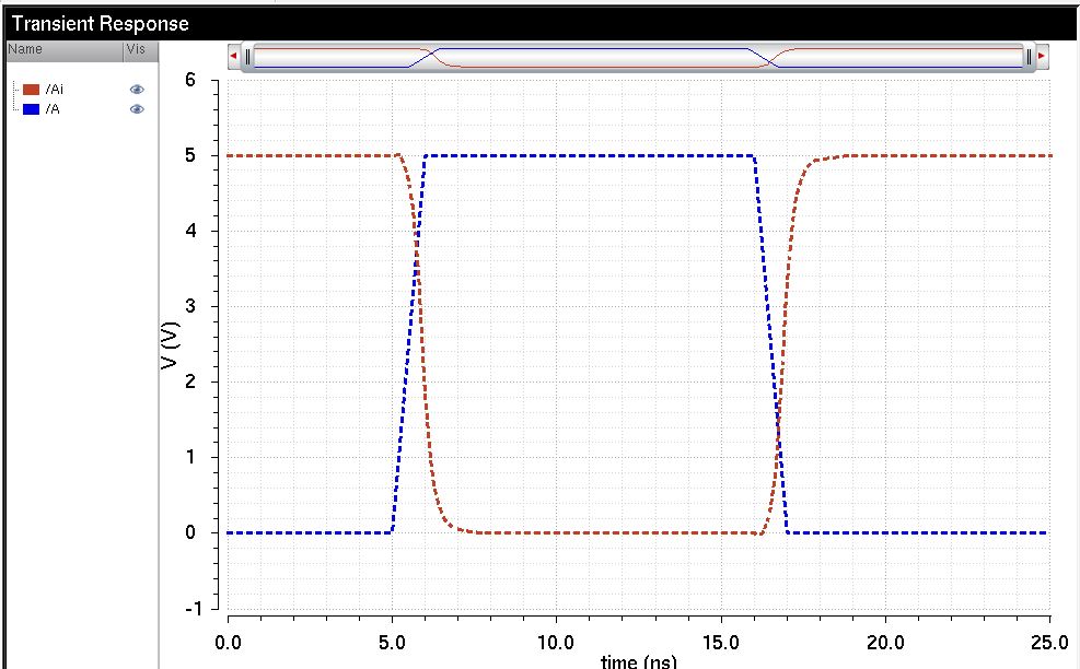
The 1pf load
12u/6u inventer:
48u/24u inverter:
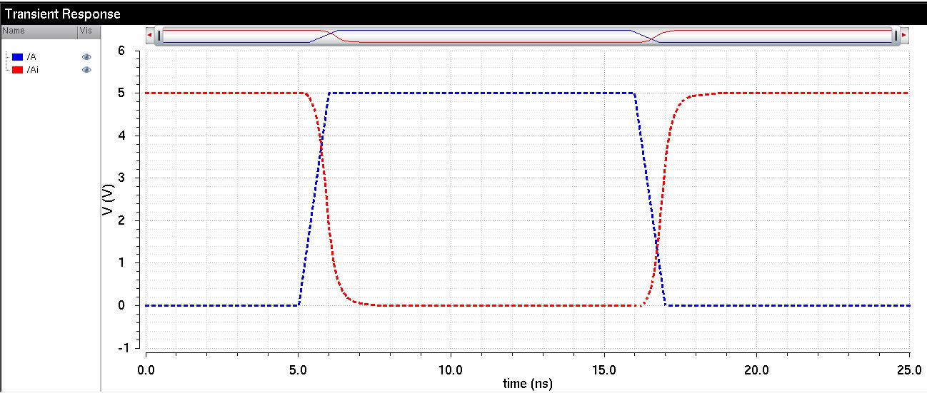
The 10pf
12u/6u inverter
48u/24u Inverter:
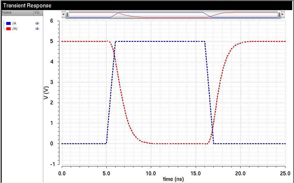
The 100pf Load
12u/6u
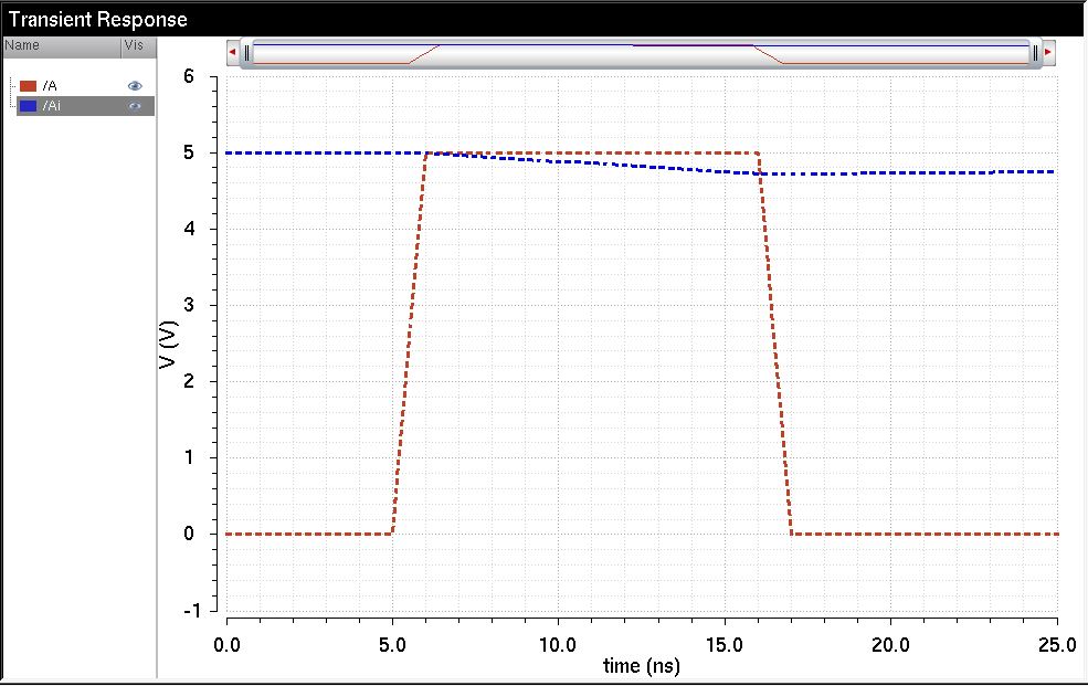
48u/24u inverter:
we should know when the capacitance is increasing it takes longer for the output voltage to
change ,and the 48u/24u inverter responcds slightly ,so its much better
than the 12u/6u inverter for larger capacitors.
we reapeat the last
simulations using Ultrasim insted of spectre.Luanch ADE-L and
->setup->simulation/directory /host and select Ultrasim from the
drop down menu,dont forget to have stand alone model libraries
The 100f F load
12u/6u
48u/24u inverter
the 1pf load
12u/6u
48u/24u
the 10pf load
12u/6u:
48u/24u
the100pf load
12u/6u:
48u/24u:
Back up design Library "Here"
"Return to EE421 Labs"