EE421Lab -Lab4
Authored
by Mari Gilligan
Email:mgill19@unlv.nevada.edu
9-21-15
IV characteristic and layout of Nmos and Pmos devises in ON's C5 process.:
Prelab:
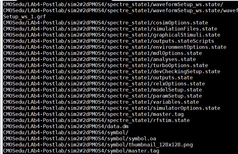
Back-up all your files and lab projects :
in
order to creat the bakup,go to Moba-x term and log in to
Csimcluster.ee.unlv.edu, when you sign in type this sentence
(tar-cvf backupdate.tar CMOsedu/).
using
this commend will creat the tar file with all projects saved.after you
creat the tar file type this commond ( gzip backupdate.tar).this command helps us to have the back up dpcuments in smaller size file.
as you can see in the window below:
after that you can use Moba-x-term to download the files to your own computerand then put it your desire file that you keep your documentrs.
Prelab4:
in Lab 4 we still will be working with tutoral1 and also going through tutorial2 .
lets
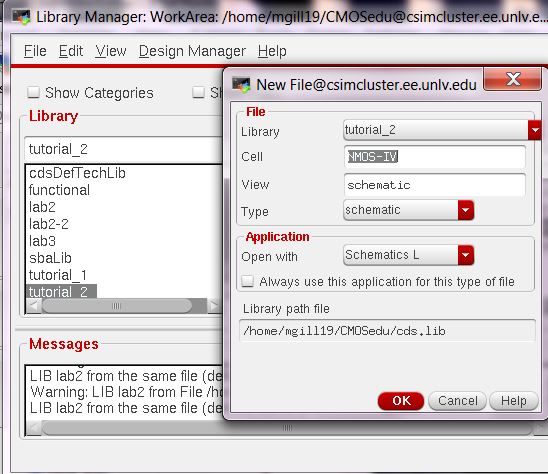
start the prelab by going to the mobaxterm and launch virtuoso,when the
library manager is open creat new folder and rename that to Tutorial
2,then
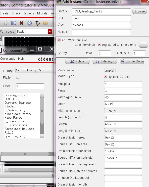
from library manager ->files->new cell view ->schematic and call it NMOS-IV .then press i (instanciate) and use the browser.choose NCSU_ ANALOG_ PARTS
and
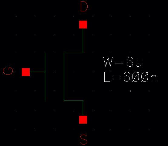
then choose NMOS3.we need to change the Width to 6um and leave the
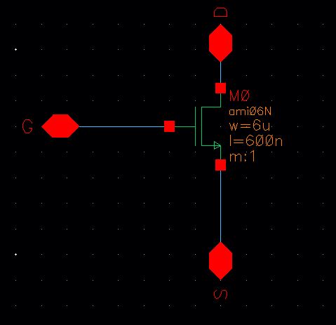
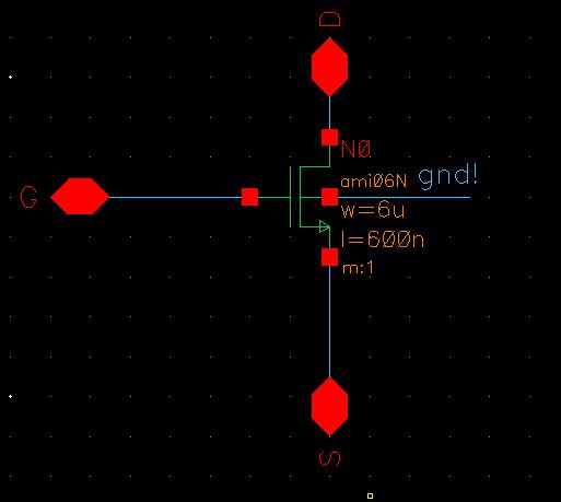
length to 600nm.place the transistor and fit the screen.you should see
the window like this:
after you place the transistor,we need to add pins(G, D,S) go to ->creat pins-> inputoutput and the add wires.righ-click on the mouse will placing the pin will rotate it,press Z to zoom and f to( fit ),m
to move and s for stretching if you need to do so.add wires with
pressing w to the pins .you should have a schematic like this:
press check and save.
we
need to creat a symbol view for the schematic.go to->create
->cell view->from cell view.when its open delet eveeerything in
the cell except the pins.since we cants see the name of the pins select
all of them and hit q->"all selected"->and display value as here:
then draw the mosfet symbol and move the pins,if you need to draw the line use create->shape->line.
add the W&L by using create->note->text.
when finish check and save.
you should have sth like this:
Next
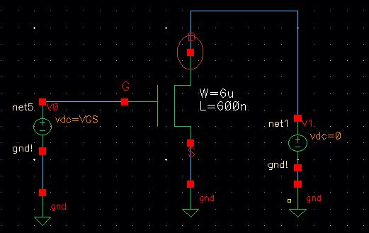
go to ->create,file->new->cell view,a cell (schematic)call
it NMOS-IV-3.then instantiate the NMOS-IV cell view make a
schematic like you see below:
set the value of V0=VGS and the value of V1=0. (check and save).
launch
the ADE,go to menue setup->Model libraries and press the buttom on
the left side ,that helps you to navigate the components you need,in
this case i navigate to
/home/ncsu-cdk-1.6.0.beta/models/spectre/standaloneand then select the
ami06N.m(nmos model )for this tutorail but notice that for PMOS we
would be selecting ami06p.m, then press open and ok.
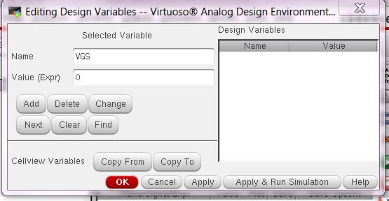
in the ADE ,select variabls->Edit->and add VGS(value for the left Dc voltage source and an arbitury value of 0.press ok .
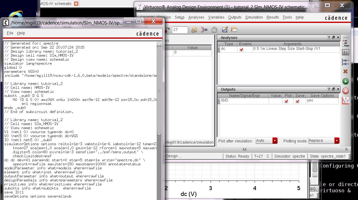
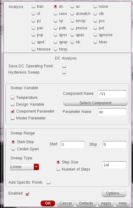
Next select Analysis ->choose and set the parameters seen below:
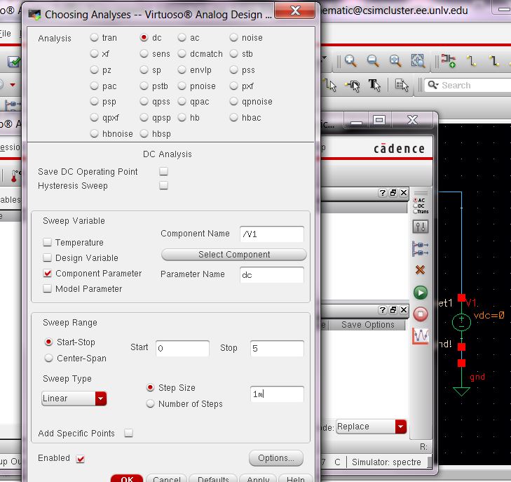
we should observe that the V1 is the right Dc voltage source and its connected to the Drain.
select output ->to be plotted ->select on schematic-> and click on the D pin to select the current .
Next save the simulation state by ->select session ->state and save in the cell view.
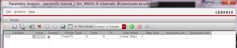
Next go to ->tools->Parameter Analysis and set the parameters as here:
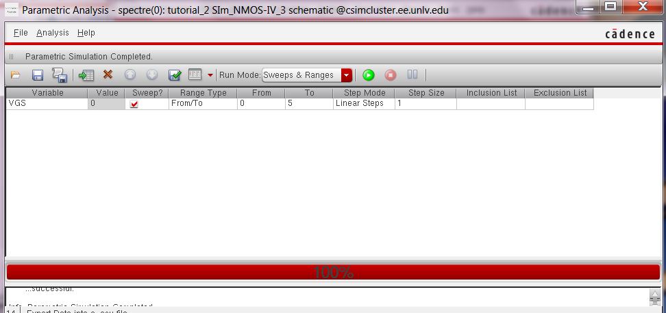
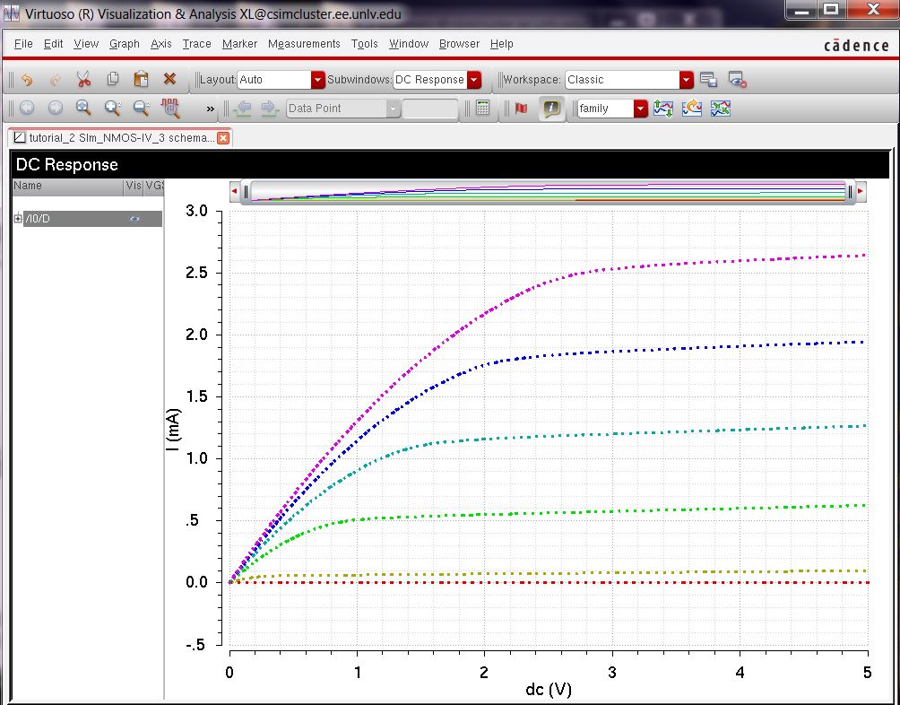
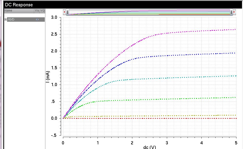
and finaly select analysis and start in the parameter analysis window.to see the MOSFET IV curves:
close the ADE window and save the state.
now
we are ready to start our Layout for (NMOS-IV-3),go to library manager
->file ->new->cell view->layout and then press fit.
when the window is open press e and set the display stop value to 10 .
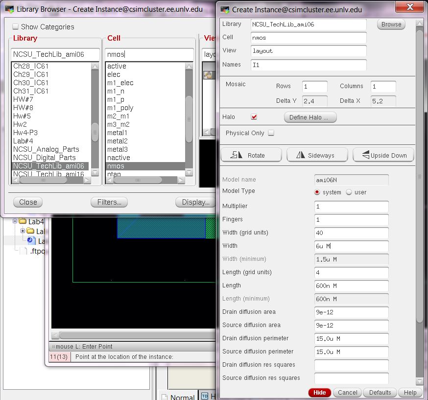
next instantiate the NMOS devise that has W=6um and L=600nm.
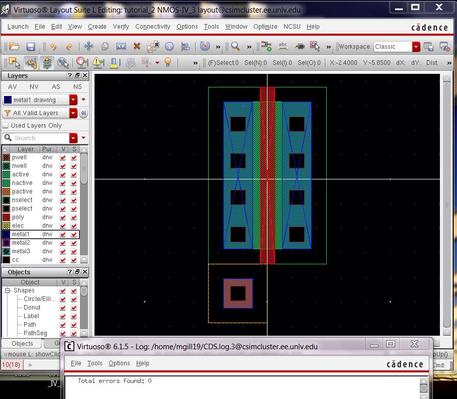
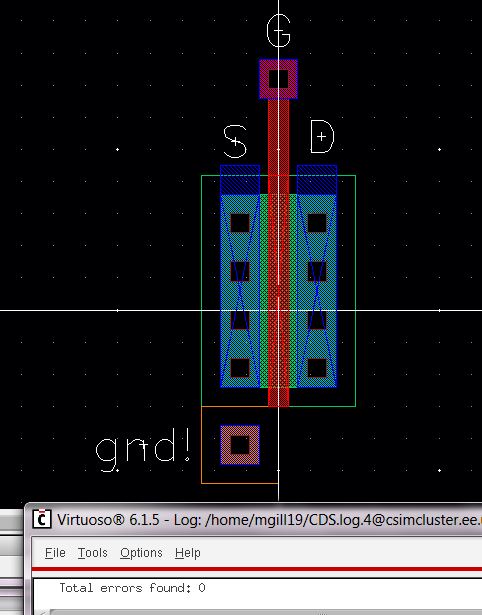
Next instantiate the Ptap cell and then DRC the layout to make sure there isnt any erros( go to verify->DRC then ok)
Next
add rectangular (press R) on the metal1 layer to connect the source to
the p-substrate and also to the drain.then add metal1 to poly cell
(m1-poly)and ass a poly rectangle to connect the gate to m1_poly.DRC
your layout.
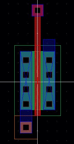
lets press e and set the display level stop =0 and we see this :
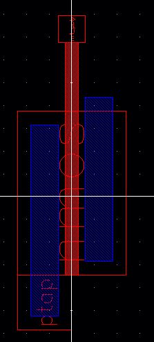
set the Display level back to 10 and add D,S,G pins on metal1,make sure you hit the "display pin name "
and I/O type i sinputout to matc the pins,nexxt draw the pins and DRC
your layout,if there is no errors then check and save your layout.
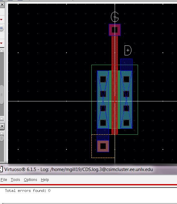
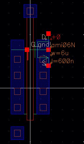
Next extract the layout and verify->extract.
then open the extracted view:
if
you pay close attention ,you will realize that the transistor has 4
terminals not 3,where its assumed the (psubstrate is tied to the GND).
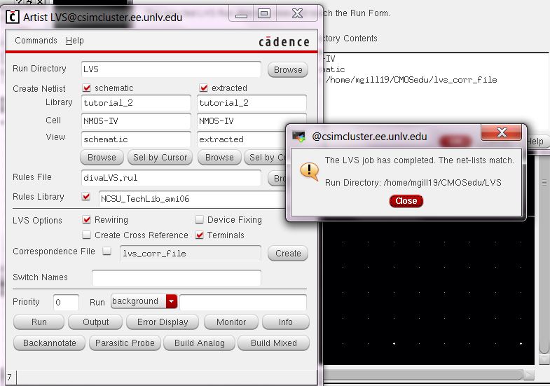
now we will run the LVS for tutorial 2(schematic vs extracted ) : and yes LVS failed .
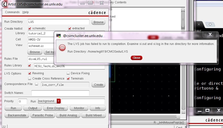
hit the output and click on the Info and then log file to get this:
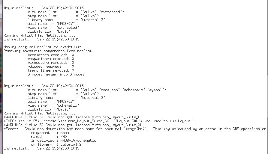
the error is from the bulk(p-sub)connected for NMOS,assumed bulk is tied to gnd for an nmos device and vdd for a pmos device.
lets
fix that by deleting the metak1 rectangle and pin connected to S to the
bilk(ptap) as below,add metal1 over the S&B metal.add pins ,again
make the pin the same size as the metal1 rectangle and add the gnd!.
save and DRC the layout.
:
now verify ->extracted,and run the extracted once again,notice that the bulk now is connected to gnd!
run
the LVS and once agin we failed,.it seems like that the LVS wants us to
use the 4-terminal transistor in our schematic ,so lets try it:
close
all the cell view and go to ->library manager->rename the
NMOS-IV_3 to NMOS-IV also rename the SIm NMOs-IV-3 to sim-NMOS-IV.
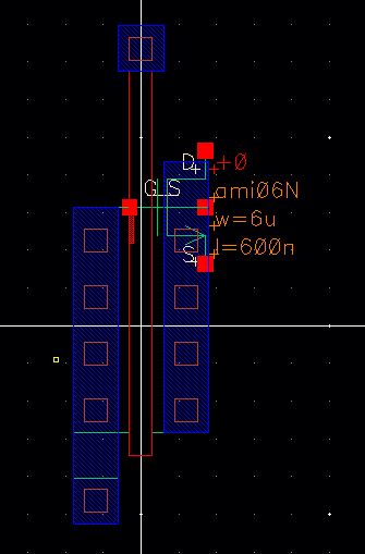
open the NMOS_IV schematic and change the NMOS symbol as bellow:
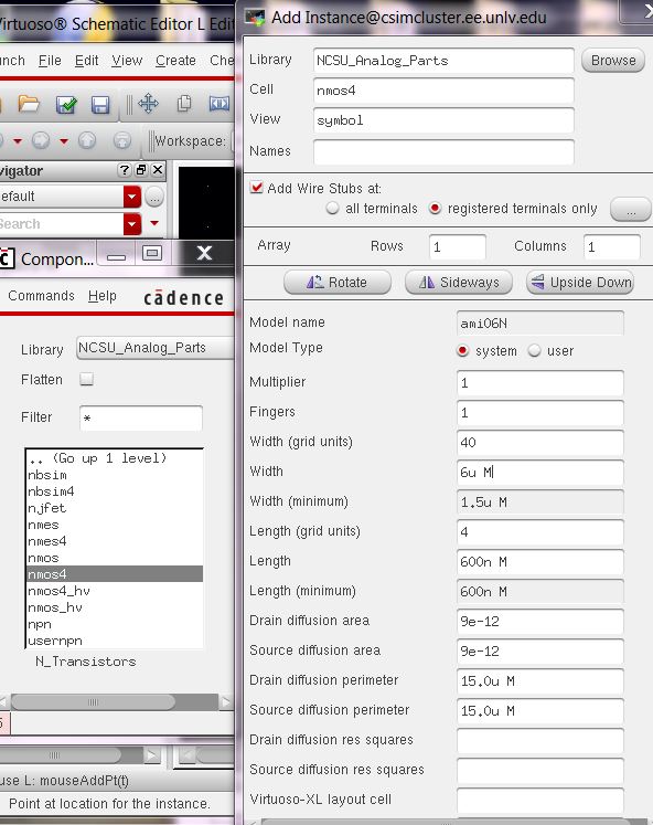
then
go to ->verify->extract ,then open the extracted view and run the
LVS'Make sure to select the correct cell: as i did here;
and yes ,my LVS matches now.
ok lets try to simulate the extracted layout.
open the schematic vieew of the SIM-NMOS-IV and then launch ADE L.
go to session -> load state->select the cell view and ok.
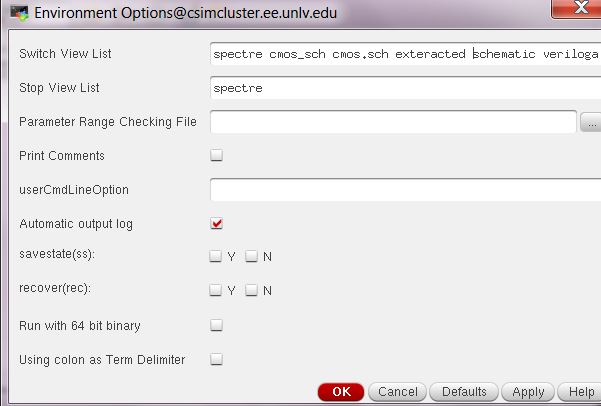
then o the ADE menu,select the setup->environment and enter extracted before schematic as you can see here:
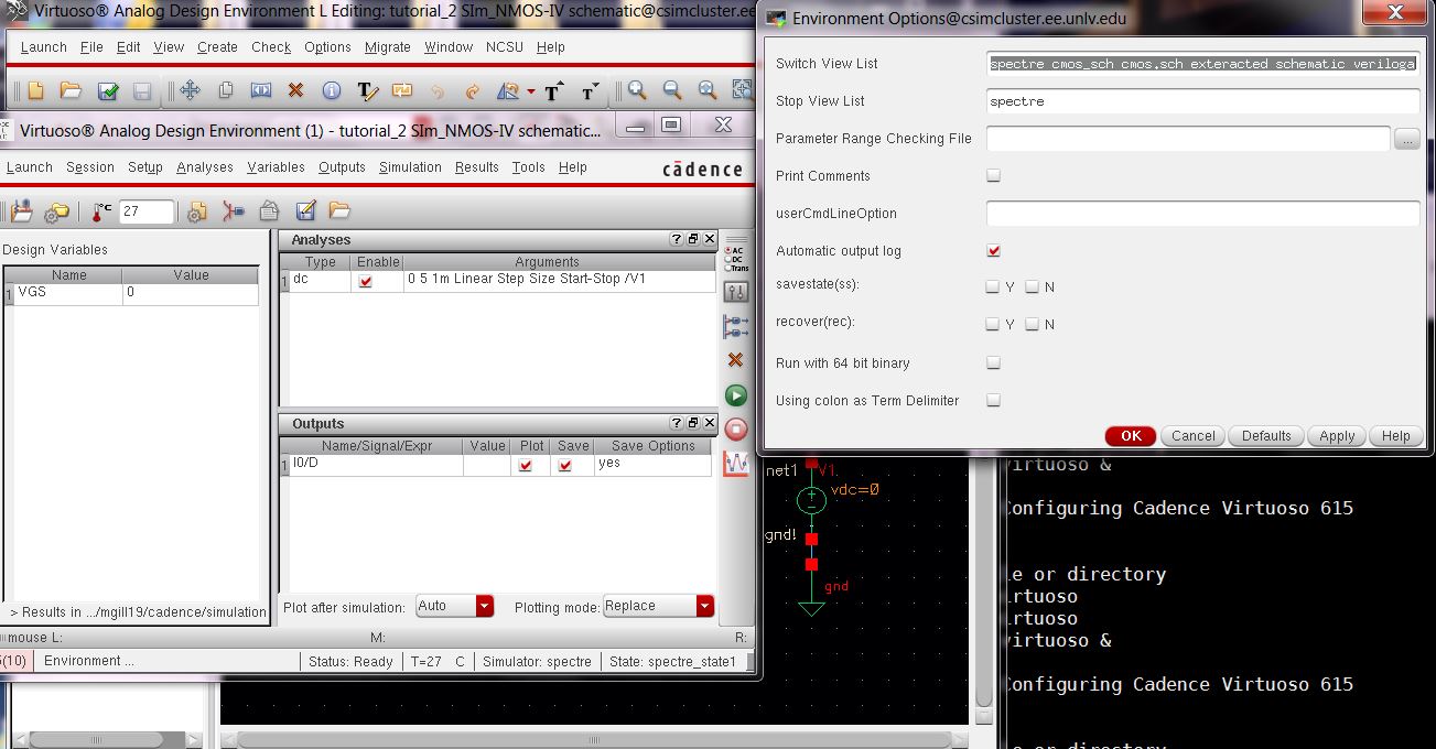
as we did earlier select tools->parameter analysis,enter the values seen below and start the simulation.
And finally the same IV curves we got earlier.
Lets go through the PMOS Devices now:
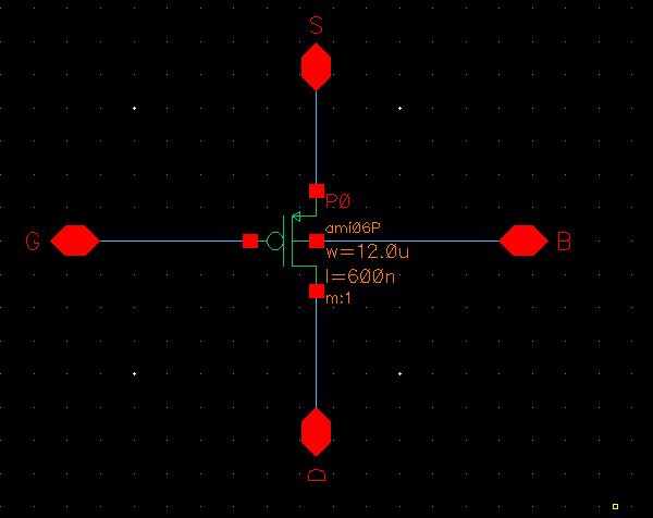
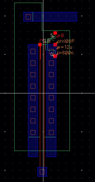
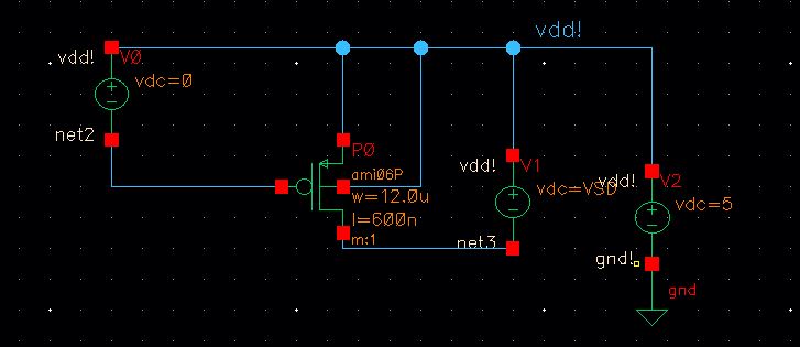
create the schematic cell view called PMOS_IV with 4 pins and set the W=12u, L=600nm and thre it is :
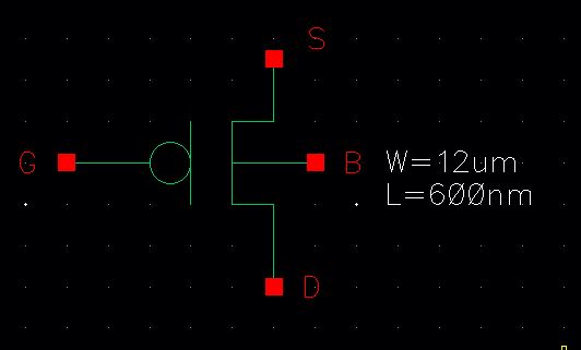
check and save your schematic and create a symbol for the schematic,Like this :
check and save the symbol ,nect creat the layout(PMOS cell and add ntap)
DRC and save the layout:it should look like this:
NExt extract the layout .open the extracted view in the Library manager.
save and close all the windows.
next create a cell and call it SIM-PMOS-IV and make the following schematic :
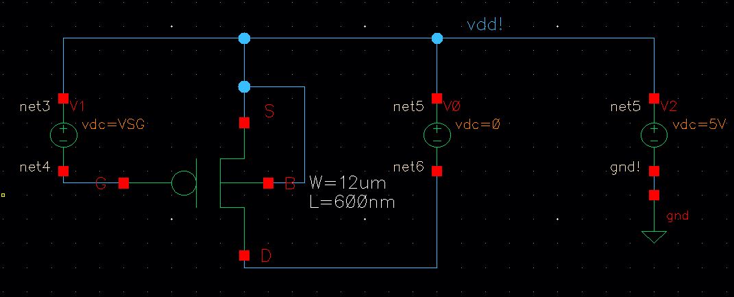
next
change the valu of V1 to VSG and check and save after that.as before we
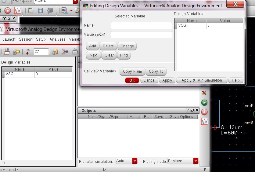
need to simulate our schematic ,so luanch the ADE and go to
->setup->Model libraries ->select the PMOS models for AMi06,go
to variables->Edit and add VSG with a value of 0(not VGS).
select the outputs and the source termianl of the transistor .and make sure that both plot and save are selected,like here:
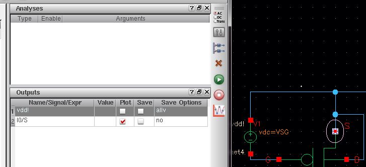
go
to analysis and eneter this:V0=VSD and VDD =V2 and really doesnt do
anything.eventhough it might be 0 but we still considere it since we
know thats very common to connnect the S/B to VDD!.
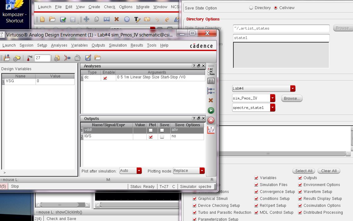
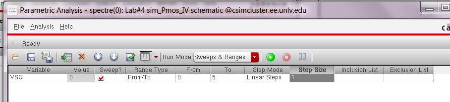
save the state and go to ->parameter analysis and then enter the values below:
start
the simulation and notice that this is a simulation of the
schematic.now we should simulate te extraxted view ,go to ADE
->setup->Environment and add extracted before the schematic,like
we did earlier. note to save the state.
and there we have the same IV curves that we got earlier :
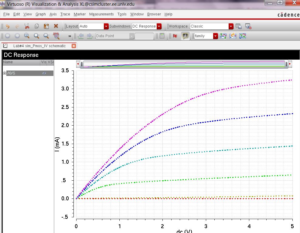
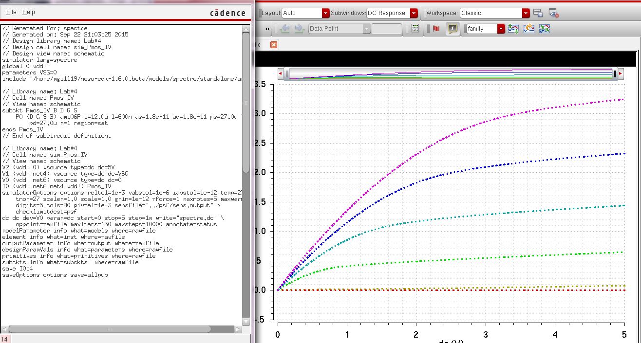
just
to make sure that we are simulating the extracted view ,go to DAE
simulation->netlist->Display.and thats what you should see.
End of Prelab
Now
we are going to create IV curves:lets start with the 3-pin
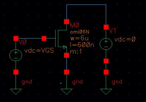
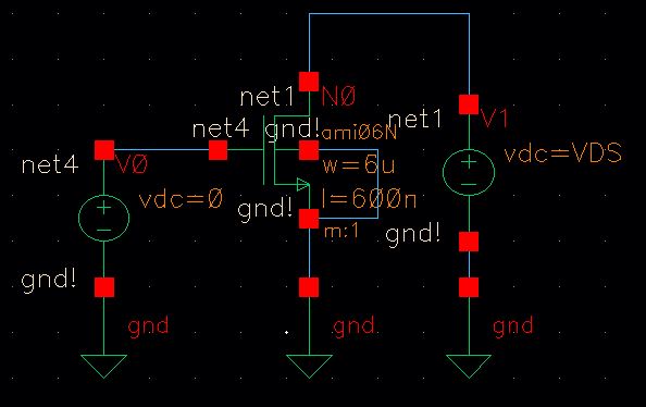
NMOS.so,create a new schematic and call it sim2-NMOS3.add pins,Here our
W=6um ,L=600nm.then add two Vdc for voltage sources and connect one to
the Drain and one to the Gate.adjust the dc voltage of the Gate=VGS,
the dc voltage of the drain=0.
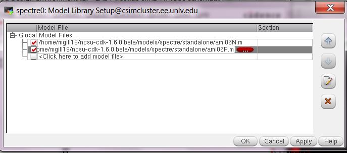
check and save and then try to simulate by going to ->ADE-L,->setup->model libraries.we should include the models ,so for that go to->NCSU-cdk-1.6.0.beta->Models->spectre->standalone.then select ami06N.m and ami06P.m.
after this go to->Variables->edit,and then you need to add VGS=0.
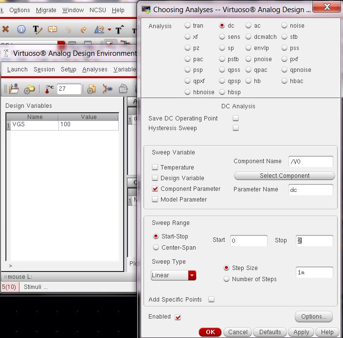
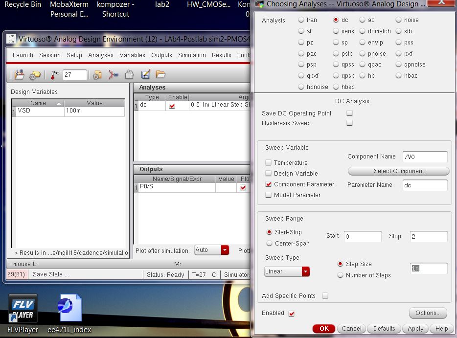
Next
choose the analysis and use dc.select the componenet parameter .as it
said in the LAb4,we are sweeping V1 ,dc value ,start =0v ,stop=5v,dont
forget to change the sweep type to linear and linear step size =1m.
go to ->outputs->to be plotted on schematic,and choose the current through the NMOs.
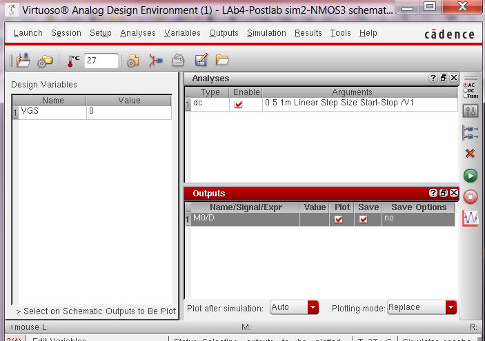
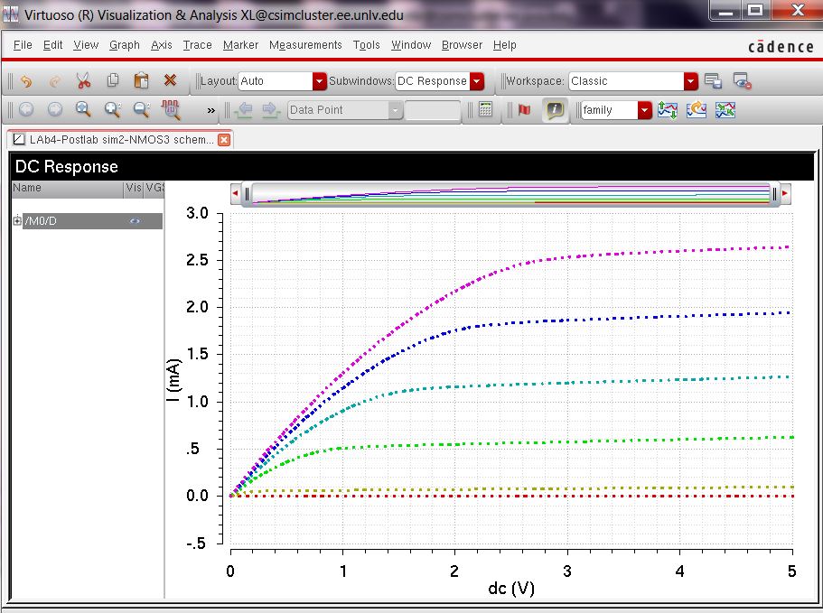
Next go to tools->parametric Analysis and follow what i did in this step:
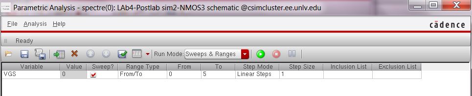
now
we are ready to do the simulation,so go ahead and hit the green button
that you see in the parametric Analysis window,you should get the IV
curves like this:
save
the state and close the window,.copy your NMOS_3 or whatevere you
called it to NMOS_4 ,after that open the NMOS_4 and do some changes
like:connect B to ground ,but keep the L,W the same size as before.now
we are going to plot IV Vs.VGS.so VDs=100mv,VGsfrom0 to2v in 1mv
steps.and change your power supplies too.like this:
Next go to -> ADE_L ->load state and make this following changes:
you dont need parametric analysis since we have only one value.
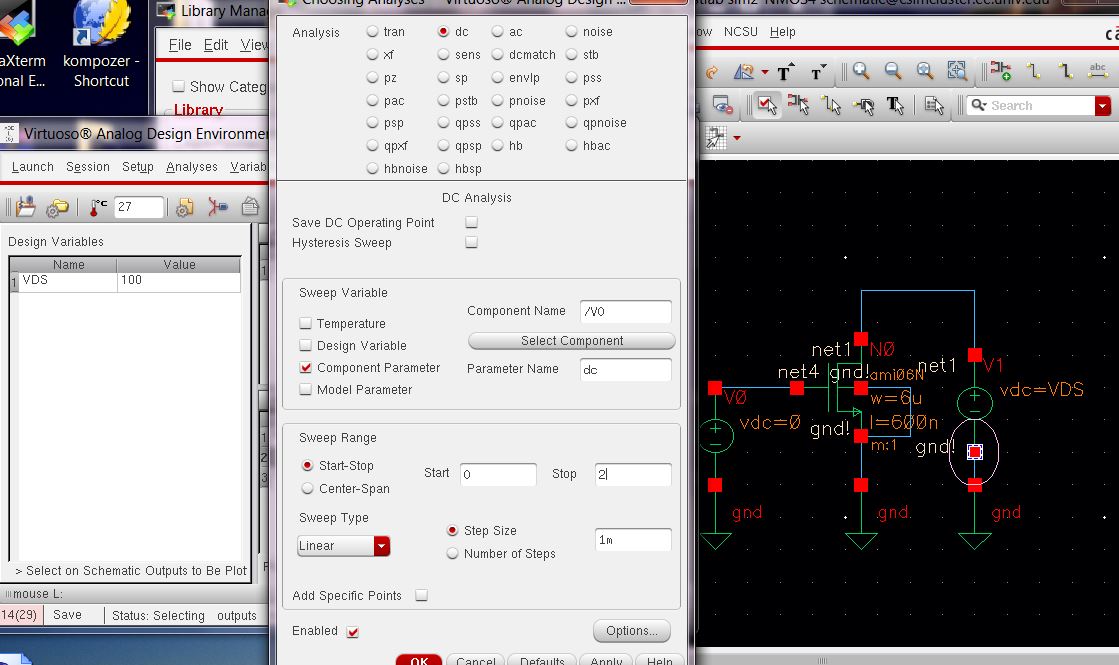
Hit the simulation button(green buttom)
and you should get this:
reapeat
the above process for PMOS,cope NMOS-3 to PMOS-3 and change the VGS to
VSG.we need another voltahe source ,so press(i) ,or instantiate ,set
the new voltage source to 5v, make sure you are changing the NMOS to
PMOS and change w=12um,but leave the L as it was =600nm.
Next
go to ->ADE-L->load state,current needs to be changes from VGS to
VSG.Run the Parametric simulation as we did earlier.
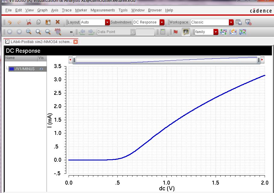
and finally we should have this :
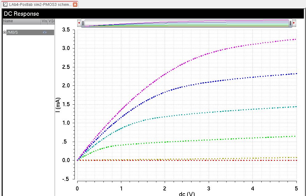
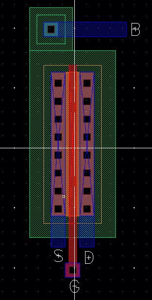
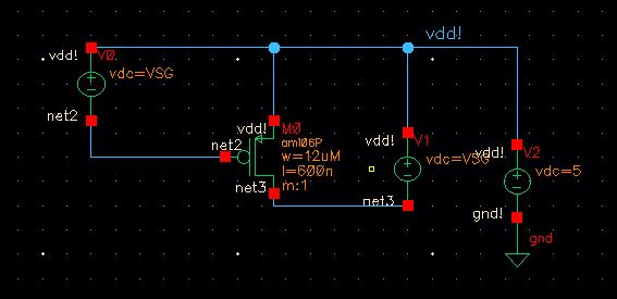
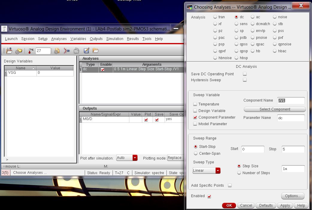
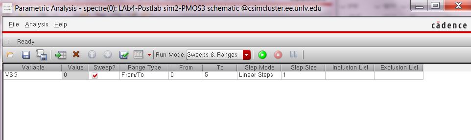
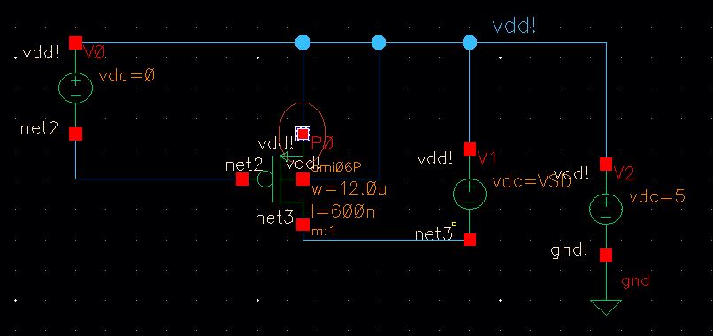
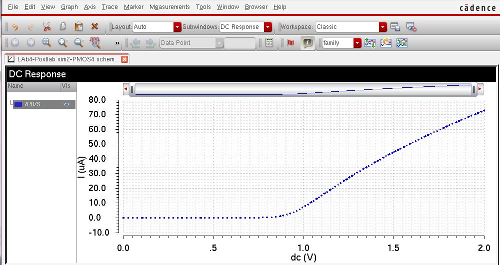
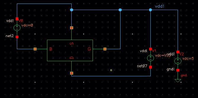
save the state,copy the PMOS-3 to new file PMOS-4,change the PMOS-3 to 4pin,connect the Body(B) to VDD.
Plot IV vs. VSG for this schematic ,VSD=100mv,VSG varyfrom 0 to 2v in 1m ,set the analysis as we did before.
and plot the P0 node ,go to outputs->to be plotted on schamatic.
and our result:
we
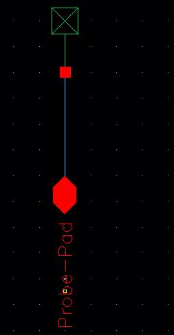
are going to creat this probe pad:so close all your prevous work after
you save them and open a new cell view,in oredr to creat this probe we
go to press (i) ,->basic->misc->noConn and add the pin :
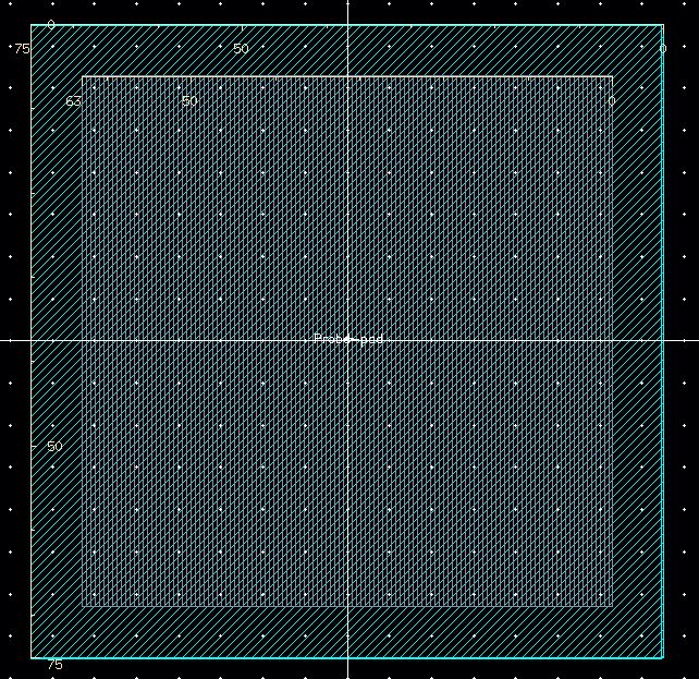
create
cell view from cell view for a symbol,and after that creat the layout
,from provous projects we know that M3=75um and glass=63um.put the
glass on the M3 and add pin.
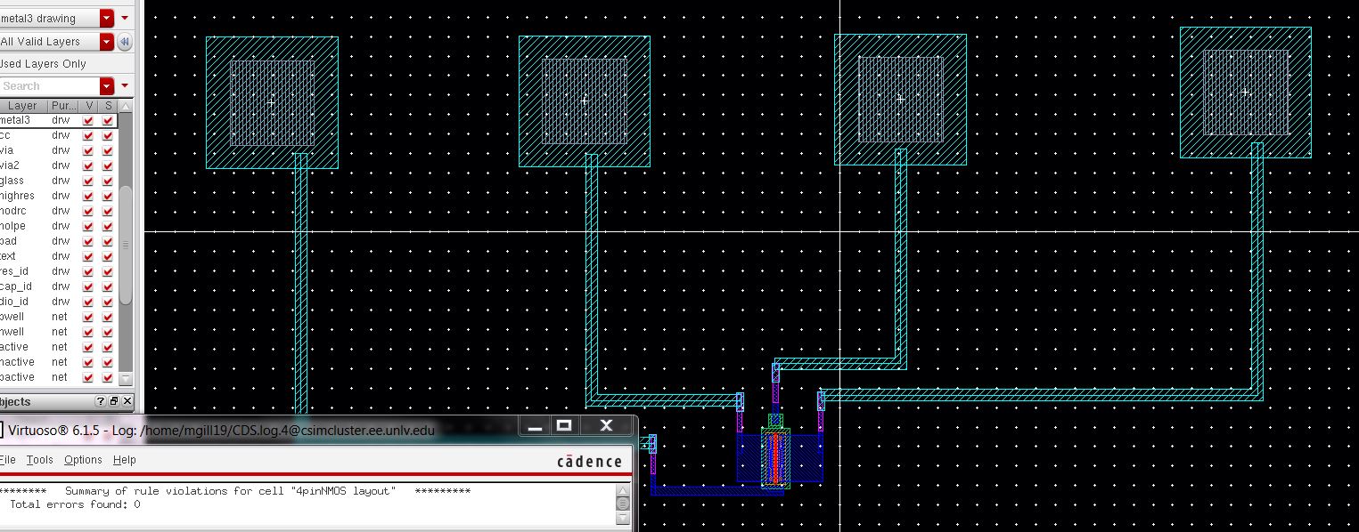
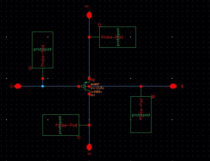
now
go ahead and creat this schematic for a 4pin nmos with probs that we
just created .we are using m2-m1,form the NCSU-Techlib-ami06 for Via1
and then we are using Metal2 to go between metal 3 of the pads and
metal1 of nmos,.for via2 use m3-m1. creat the symbol and layout
as well.
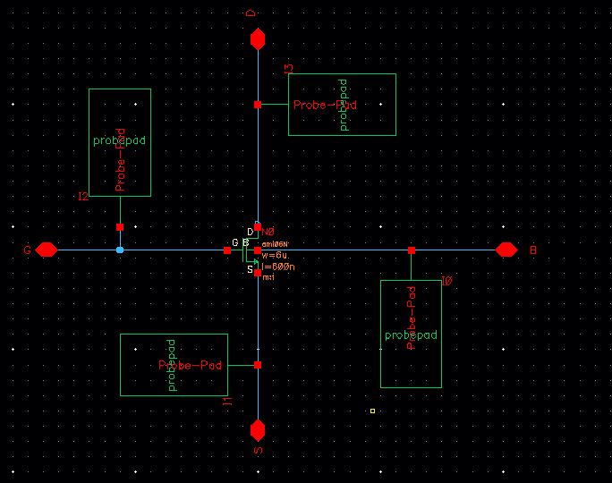
connect them like this : and do DRC,
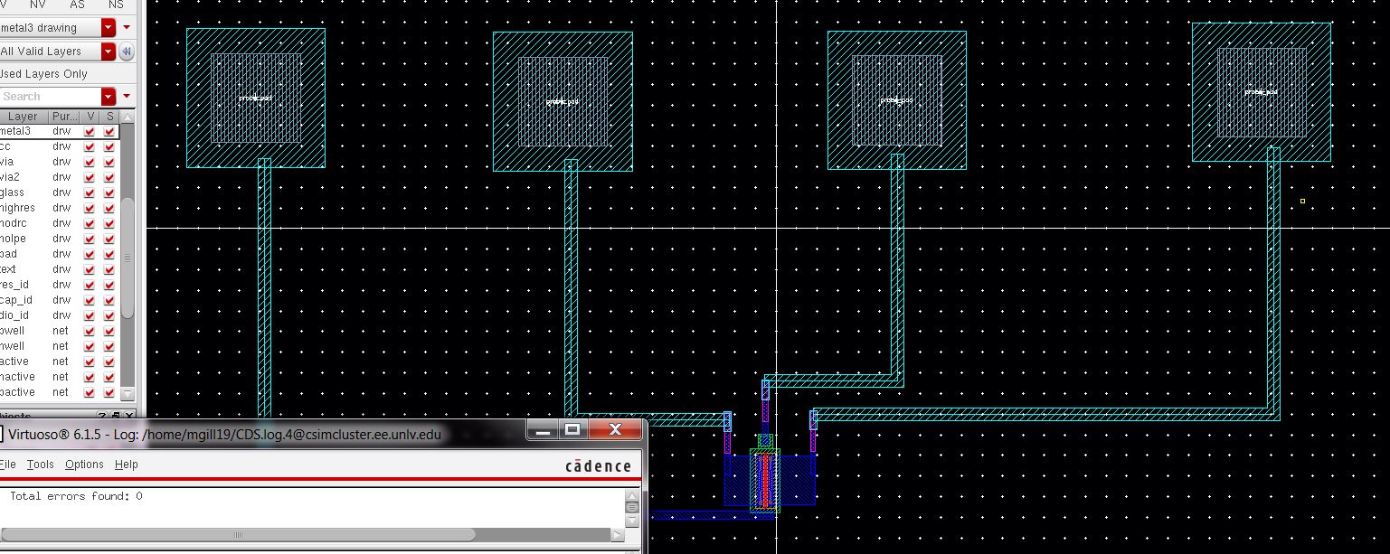
do the same thing for PMOS4 as you did for NMOS4
connect the pads and run the DRC:
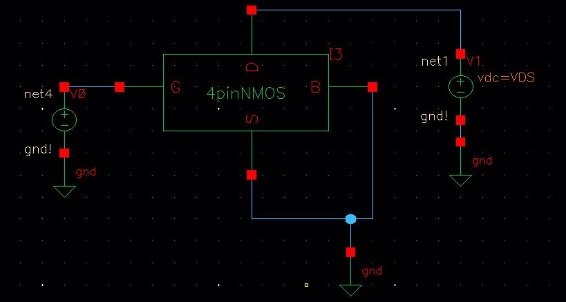
now i need to have schematic for running the I-V curves for each one:
End of Post Lab
Backups are located "Here"
"Reture to EE421 Labs"