Lab 3 - ECE 421L
afetr you see the bakup file,backup.tar in mobaxterm then download the file on your own pc.
finally upload the file to googledrive or dropbox.
go to CMOSedu and creat a new folder name Lab3
log in to mobaxterm and launch virtuoso &.
in this lab we are using lab1 and tutorial1 .open the symbol for the divider that we had in lab1.
we need need to make some changes in the symbol ,so go to creat -> shape->line and change it to the figure that i have here:
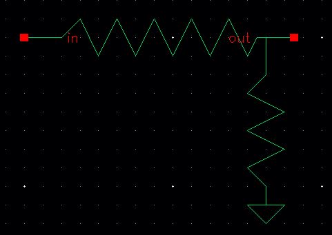
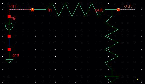
Dont forget to check and save the symbol. now we are going to remove the divider from schematic and redraw with the new symbol that we just created.
luanch ADE L and load the previous state..we are ready to run the simulation and we will see this results:
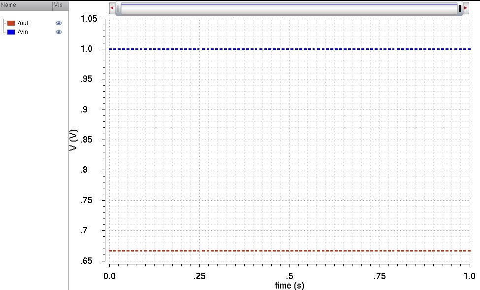
after seeing the simulation results, we know the symbol works and we are going to make the layout.
go to mobaxterm and luanch virtouos ->go to library manager and select the R10k or wathever you called it, go to file->new->cell view and then select layout ,you will have this:
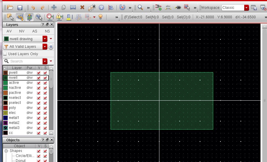
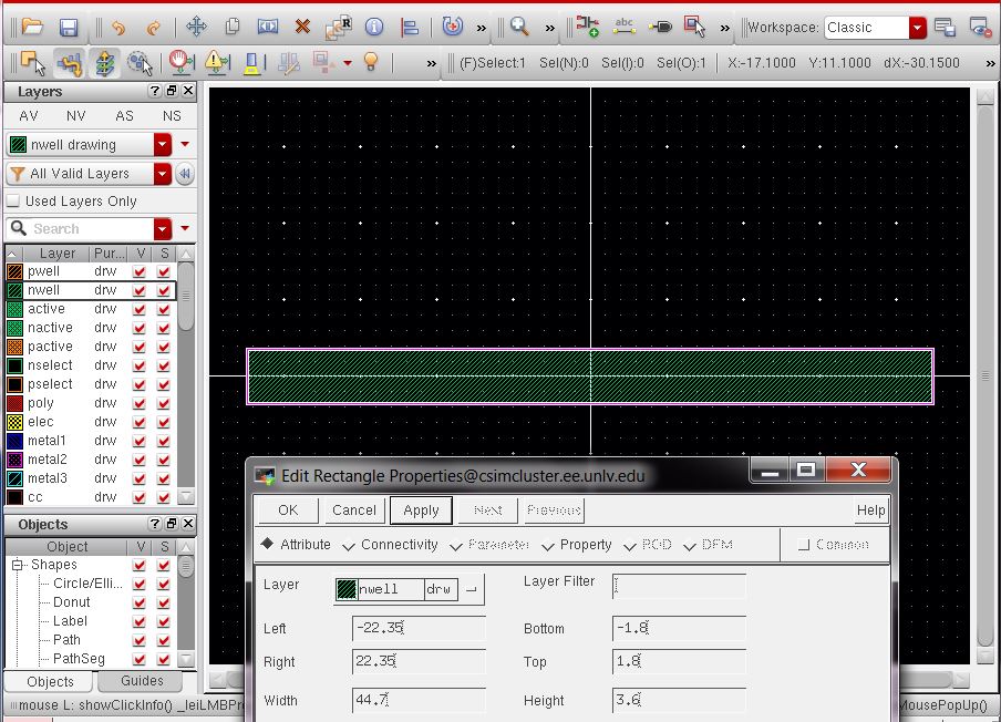
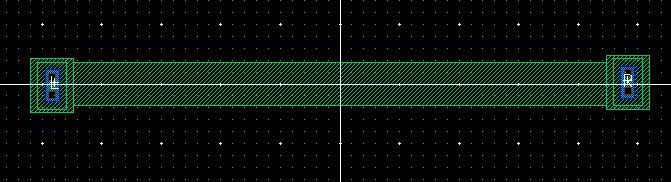
I alredy picked n-well ->R for the rectangular on the layout.then we will creat the 10k resistor .the sheet resistor is 808 ohms,so the L/W ratio is approximatly 12.4(CMOSEDU design rules) and the min width is 12 lambda.Explaination :L=148 Lambda and in this process lambda =0.3 um. after calculation the layout needs to be 44.6um for L and 3.6um for W,but in order to use lambda 0.3um we need 44.7um for L.select the rectangular and press Q,and set the W&L and you should get this:
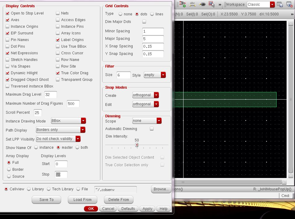
dont forget to type e and change the display level to 10,and then select the pin names like below:
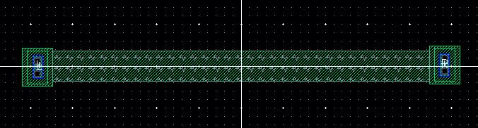
now its time to add taps and place them onto n-well.this can be done by going to press i on the page nad go to NCSU-TECHLIB-amio6 and select ntap from there.i choose to rows for the cnotacts ,place them onto end of the n-well.
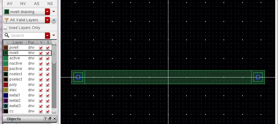
go to Creat->pin and select metal1 and type L for pin name,select the terminal name and placed that on the top of left ntap,do the same thing for right side of the n-well as well.
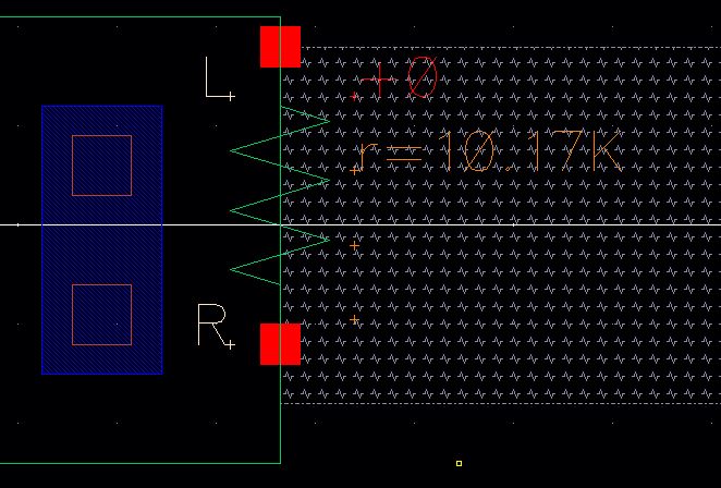
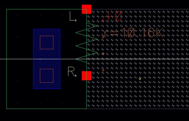
then select res-id to add the idenification resistor to n-well.do the verification through ->verify ->extract to see the resistor value of the n-well.->library manager ->extraxted view and zoom in and you will see this:
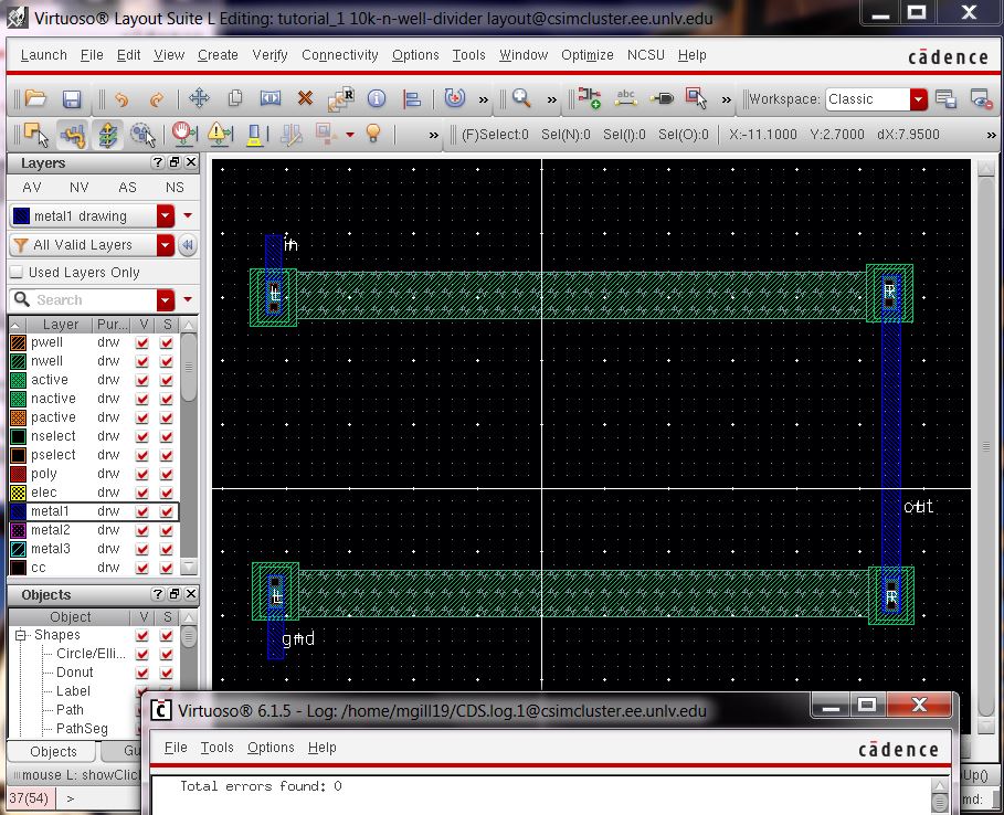
finally create the layout of the divider symbol ,go to library manager to have a new layout in the cell view with the symbol we had earlier.the select the metal1 and add over the pins like this:
then DRC it to make sure you didnt make any mistakes during the design .
we ahave 0 errors.
after the DRC we need to LVS the extracted view and we might have some errors.
yes i got 2 erros for gnd which i changed to gnd! and in was inputoutput which i change it to input,.so i run the LVS again and i have 0 errors.
in the prelab iwanted to got 10k and ill have W=3.6um ,L=44.6um ,we need to place the n-taps and pins ,make sure to change the display to 10 as we did earlier.ntaps=4.5um high and i need to chnge the ratio of L,W,so W=4.5um,L=55.7um in order to get 10k and have a lambda of 0.3um .
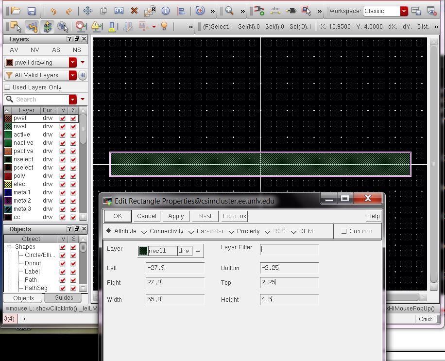
put the Left and Right pins and add the res-id layer and run DRC.
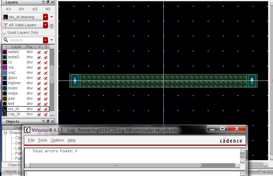
now extract the file and open the extracted file and notice that r=10.16k which is close enough to 10k.However the value of the extracted resistor doesnt really matters in the DAC.
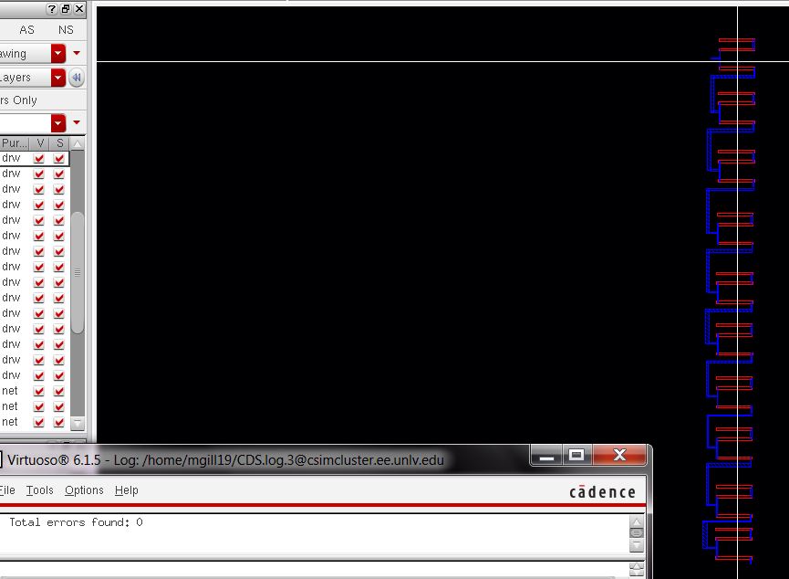
here i got the extracted view of my DAC unit with 0 errors.
now we will run the LVS to make sure the DAC unit matches up with the schematic DAC unit.
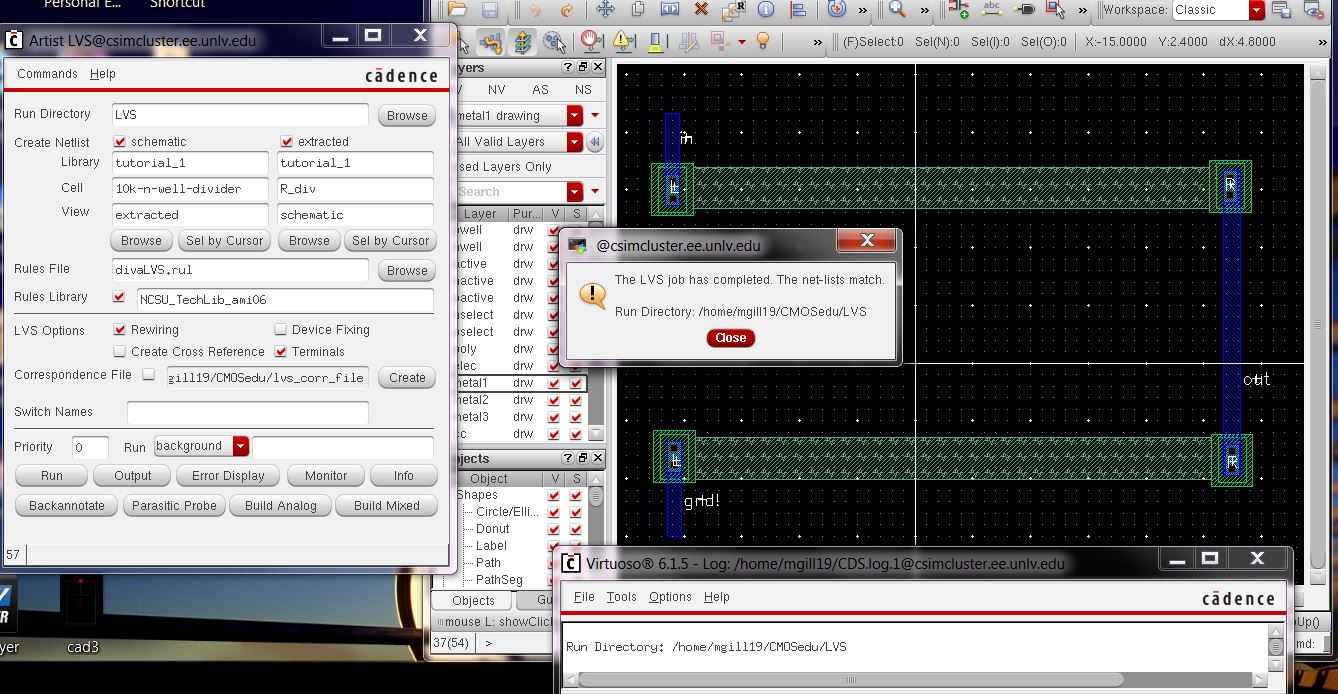
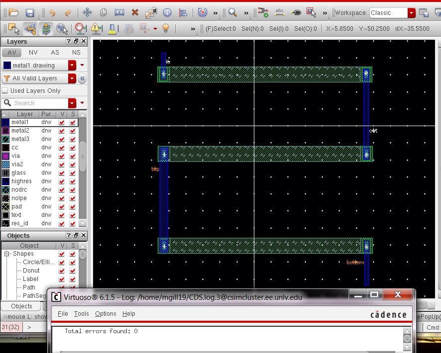
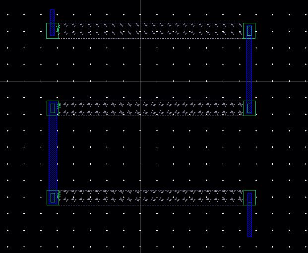
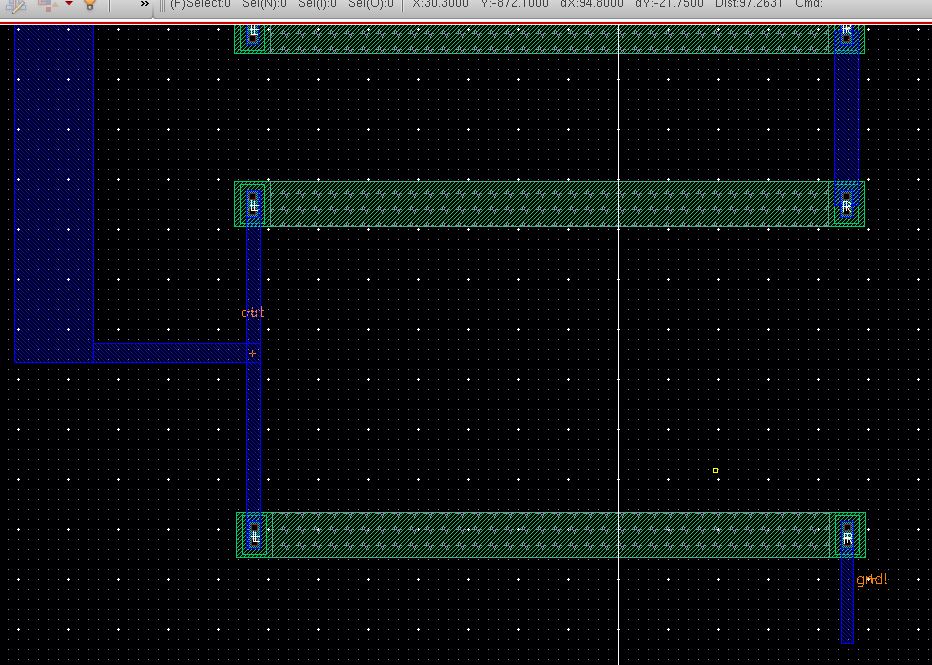
and so now that they match we know everything is been set up properly.and i can add the 1unit DAC to build the 10 bit DAC by putting them parallel on top of each other and conncet them
by metal1 layer ,output(bottom ) of one DAC goes to input(top) of the anotehr DAC below itself.when you are done connecting them run the DRC,after DRC with no erros ,we are ready to creta the extract file like this: and run the DRC.
since i couldnt get the whole 10bit DAC unit in my picture,this is a closer look to the 10-bit DAC to show exactly who i connected the bottome of my DAC.
why im showing the bootom part to you?because the top and the bottomg of the DAC are different becaue we have VOUTand GND! on the bottom part of the design ..
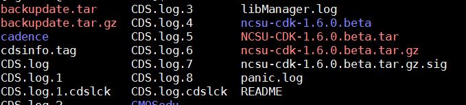
My Lab3 folder along with all of my backup files on my Desktop:
backup documents"here"