Final Project - ECE 421L
Authored
by Mari Gilligan
Email:mgill19@unlv.nevada.edu
11-08-2015
Lab description:
- Design of an 8-bit resettable (input "clear") up/down counter
- The outputs of your counter should be buffered before connecting to a pad
- A 31-stage ring oscillator with a buffer for driving a 20 pF off-chip load
- NAND and NOR gates using 6/0.6 NMOSs and PMOSs
- An inverter made with a 6/0.6 NMOS and a 12/0.6 PMOS
- Transistors,
both PMOS and NMOS, measuring 6u/0.6u where all 4 terminals of each
device are connected to bond pads (7 pads + common gnd pad)
- Note
that only one pad is need for the common gnd pad. This pad is used to
ground the p-substrate and provide ground to each test circuit
- Using
the 25k resistor laid out below and a 10k resistor implement a voltage
divider (need only 1 more pad above the ones used for the 25k
resistor)
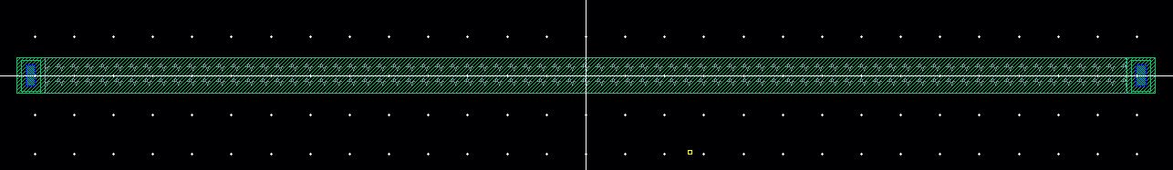
- A 25k resistor implemented using the n-well (connect between 2 pads but we also need a common gnd pad)
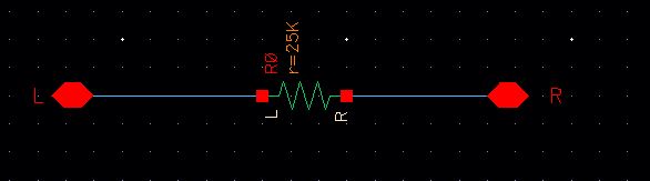
25
K resistor :
25Kresistor_symbol:
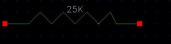
25K,resistor layout
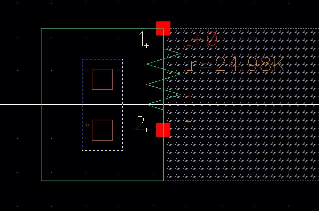
Extracted view to see if we have 25K,resistor:which is 24.98K that is close enough to 25k.
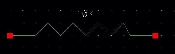
10K
resistor:
and
10K resistor symbol:
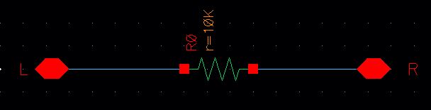
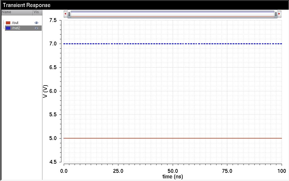
Voltage divider for 25K and 10K resistors:
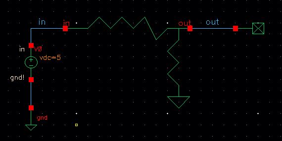
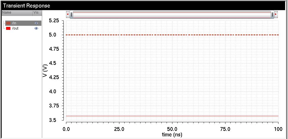
simulation of voltage divider:
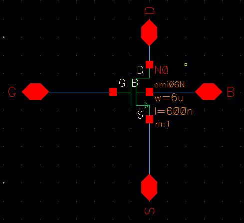
NMOS transistor schematic :
Simulation Schematic with symbol of NMOS :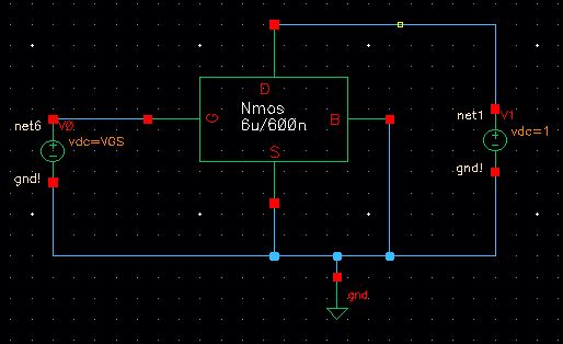
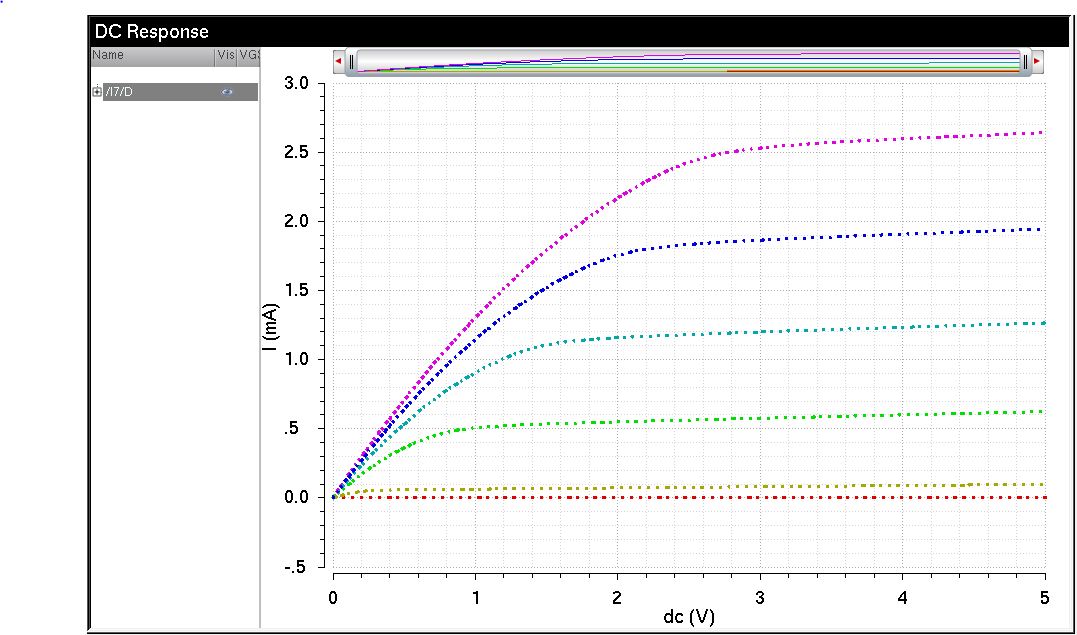
IV chractrestic view of NMOS(ID Vs VDS):
which simply means that we are varying VGS.
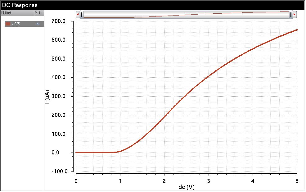
ID Vs VGS charactrestics:
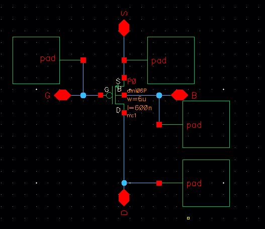
PMOS Transistor:
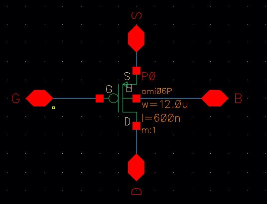
PMOS with Pads connection:
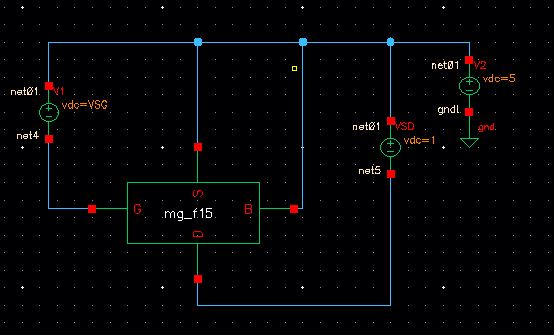
PMOS schemtic for simulation:
PMOS Schematic resualt:
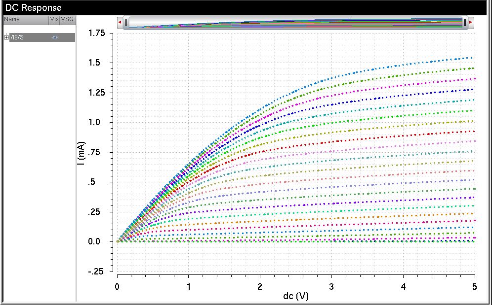
IV charactrestic curve for 6u/0.6u PMOS Transistor :

Inverter with 6u/0.6u NMOS and 12u/0.6u PMOS:
simulation of Inverter:
Transient simulation setup process for our inverter:
Inverter simulation results:
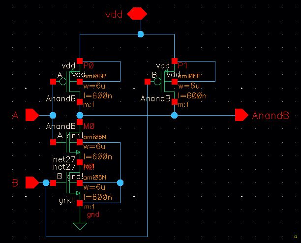
NAND Gate Schematics:
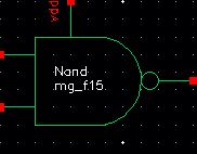
NAND Gate symbol:
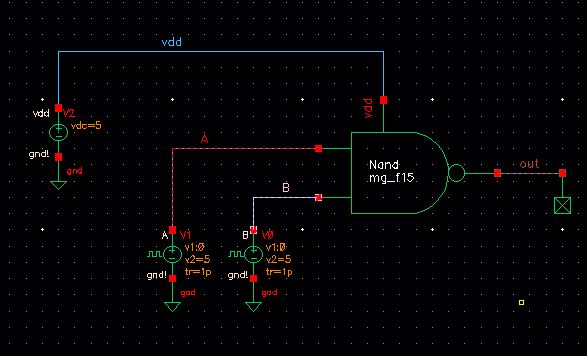
Schematic view for simulation the NAND gate:
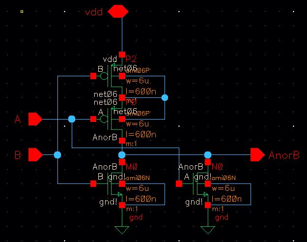
Schmetic view for simulation NOR Gate:
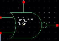
Nor Symbol:
Design schematic configration for Nor Gate: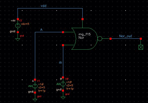
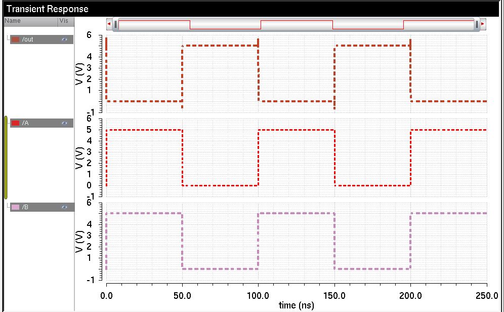
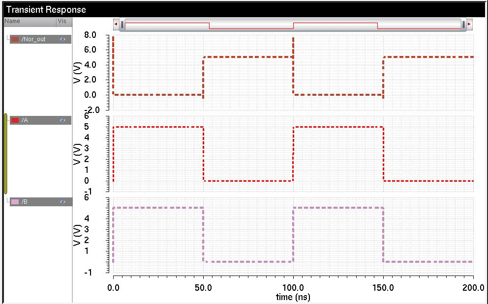
Simulation results:
Ring Oscillator Schmetic:
Arrayes
for the buses is implememented in the previous lab ,30 connection
between 31 inverters.we use the common VDD as an enable .we can verify
our frequency of the ring oscilator which will be 170MHz according to
my results.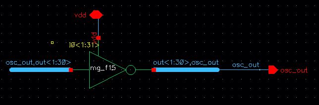
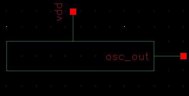
ring oscillator symbol:
Simulation of Ring Oscillator:
operation of ring oscilator by seting the osc_out to zero.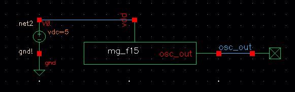
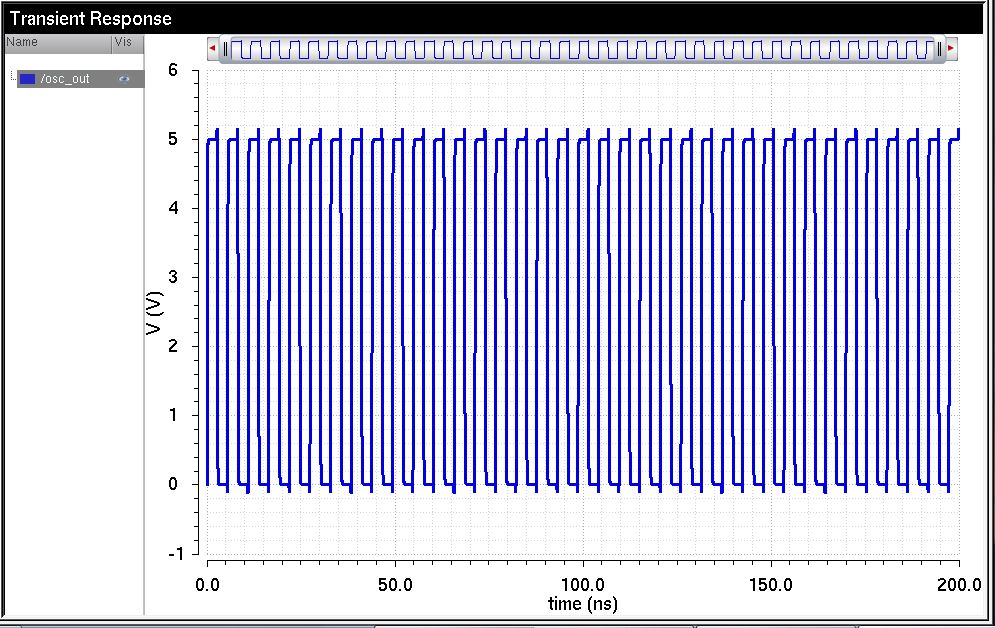
Ring Oscilator simulation results:
counter:
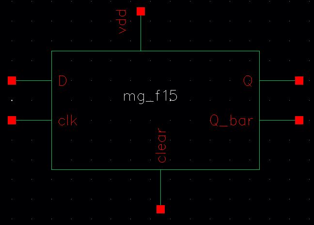
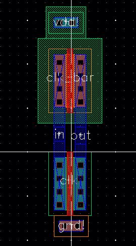
8_bit Resettable DFF:
which
is the block for building the up/down counter with the clear.this
schematic is the latches impleamented together.the fisrt latch store
the input when the clock goes down and it will send it to the next
stage when the clock changes to high.our clear input is build with with
two inverter with NAND gates.when the clear is low ,NAND gates behave
like an inverter.and when its high it makes the Q value to be
zero.without caring zbout previous stored value in the latch.the first
latch output is zero ,so this value passes when the clear is set back
to low.and our clock involves two inverter (Buffer)for not having extra
connections.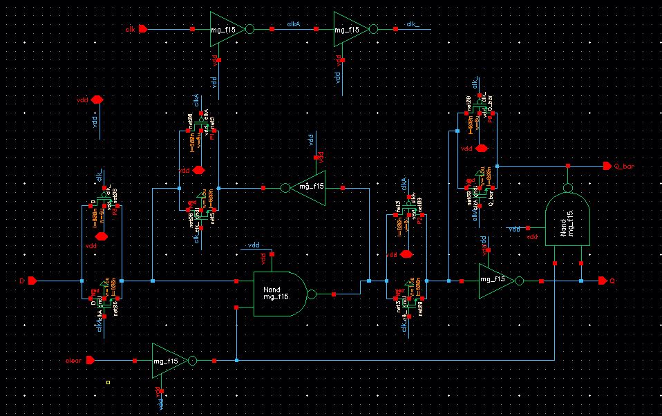
8_bit DFF symbol:
8_Bit Up/down Counter:
I
am using the symbol thar i made from my DFF and put that in the
configration below to make an UP/down counter,using the Mux for
chossing to count up or down, and Buses to make a 8_bit counter to test
the DFF .
when clear is high the output Q is set to zero and Q_bar is high.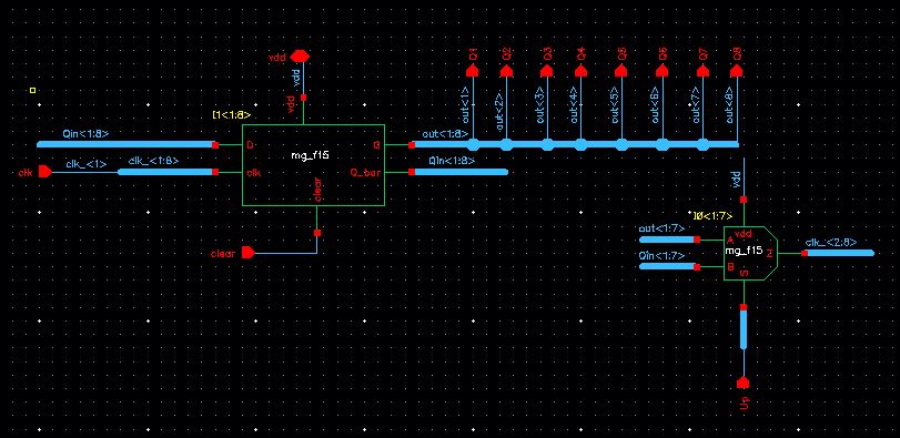
Counter symbol: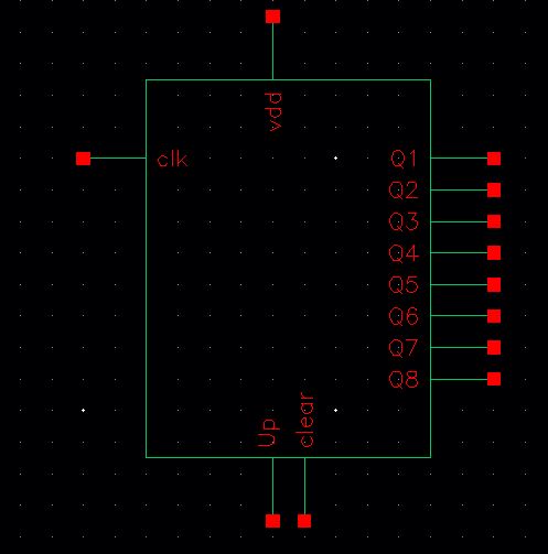
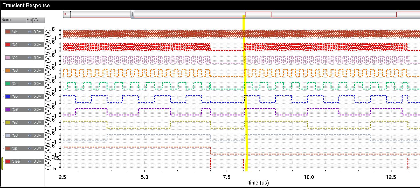
Counter simulation results:
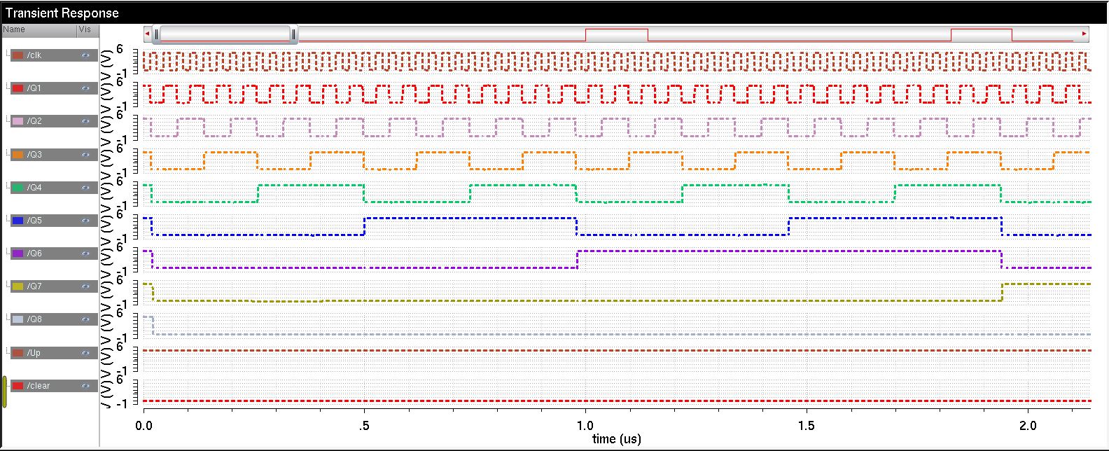
reset to zero:(yelow lines)
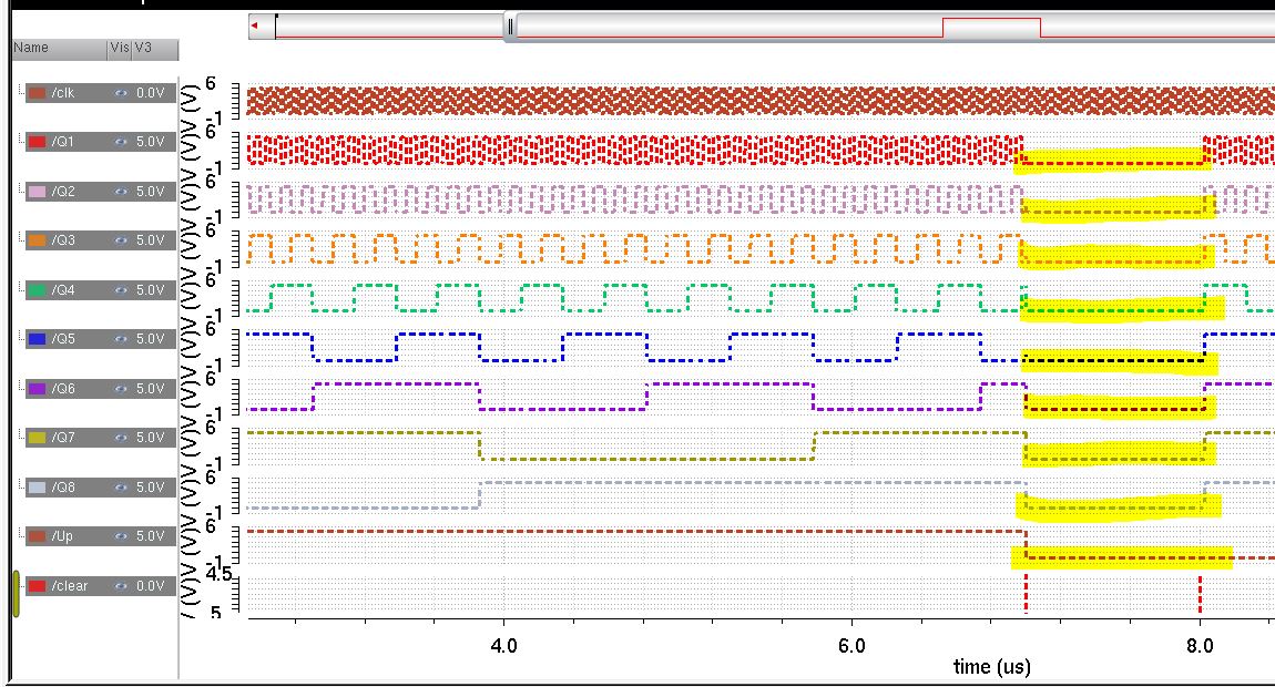
Now Count down :
Buffer Design Configration :
How to make the Buffer to drive 20 pF off chip capacitance,so the Buffer is implemented to reduce the time delay.
after
a calculation we are using 6 inverters which schale of A for each
inverter.Or another way that we can make this configaration is using
two inverters with multiplier=6.that way we will have a less
complecated circuit to layout.
Looking back to my design if
we pay close attention wp/wn=12u/6u,which gets multiply to A which i
calculated and gives a value for the nect inverter and so on....
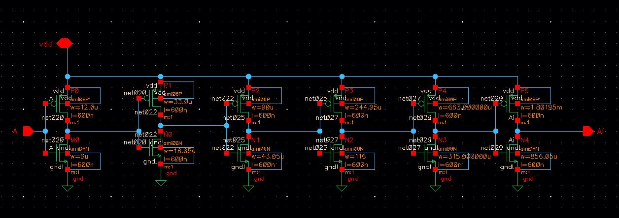
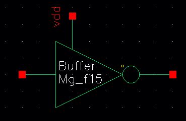
Buffer symbol for above design:
Design of schemtic of beffer to srive a 20pF off_chip cap:
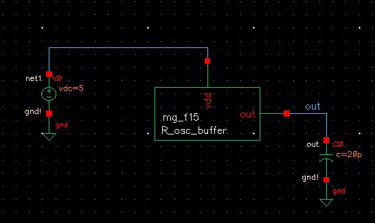
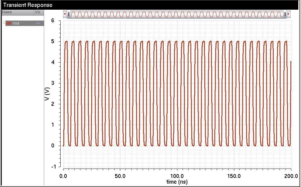
Buffer with sriving 20pF cap results :
single Buffer schematic:
this schemtic designed to test if the buffer works :
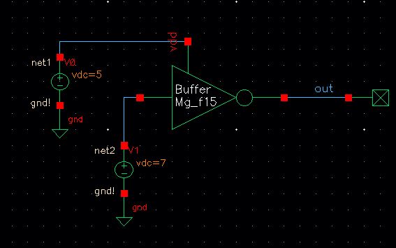
results shows our buffer works.
Part 2 of the F_15 Project Layout & extracted view of the above schemtic designs
----------------------------------------------------------------------------------------------------------------------------------------------------------------------------
Design of an 8-bit resettable (input "clear") up/down counter - The outputs of your counter should be buffered before connecting to a pad
A 31-stage ring oscillator with a buffer for driving a 20 pF off-chip loadNAND and NOR gates using 6/0.6 NMOSs and PMOSsAn inverter made with a 6/0.6 NMOS and a 12/0.6 PMOSTransistors,
both PMOS and NMOS, measuring 6u/0.6u where all 4 terminals of each
device are connected to bond pads (7 pads + common gnd pad) - Note
that only one pad is need for the common gnd pad. This pad is used to
ground the p-substrate and provide ground to each test circuit
A 25k resistor implemented using the n-well (connect between 2 pads but we also need a common gnd pad)Using
the 25k resistor laid out above and a 10k resistor implement a voltage
divider (need only 1 more pad above the ones used for the 25k resistor8-bit resettable (input "clear") up/down counter
Lets strat with the layout of each component :
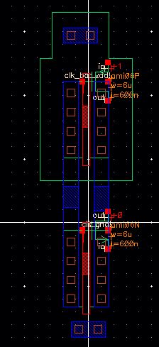
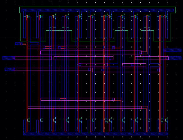
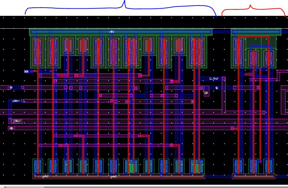
Now this is the DFF Layout and extracted view:
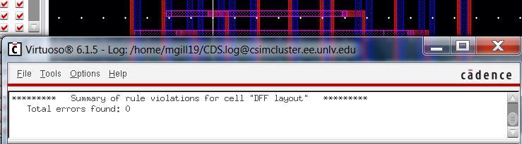
Extracted view of the DFF:
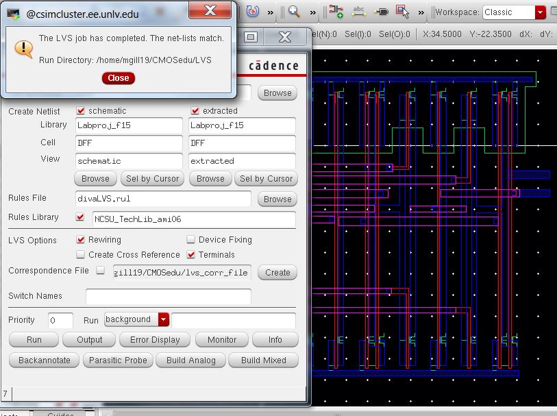
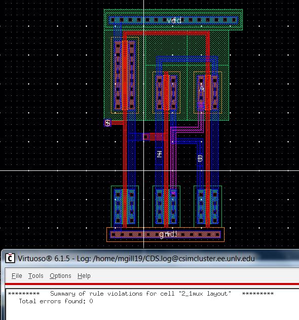
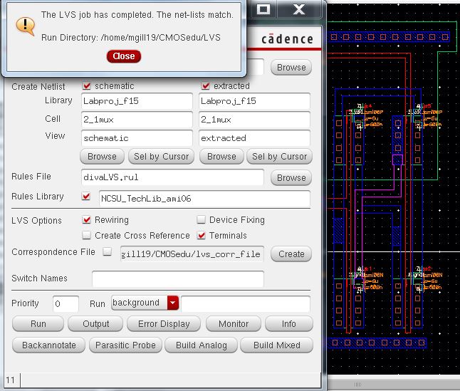
2_1 Mux Layout and extracted view:
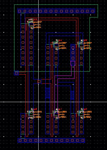
2_1 Mux LVS:
Closer look to the layout of the DFF with Mux:
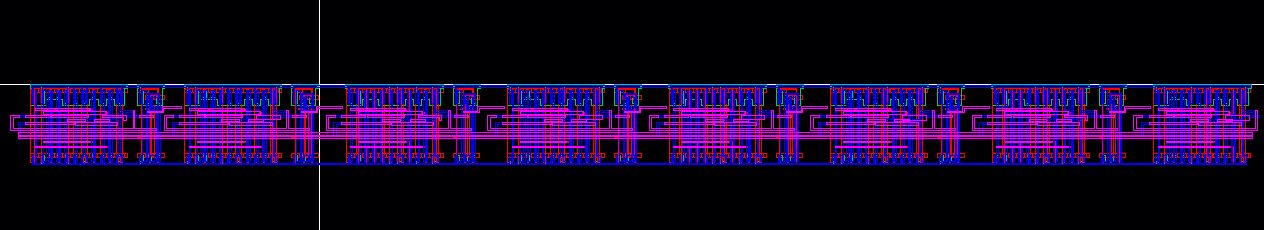
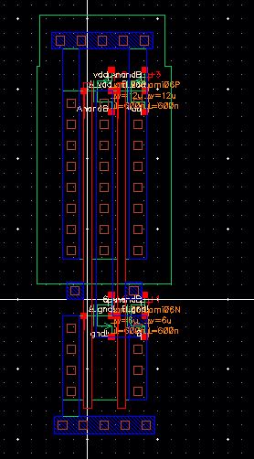
8_bit Counter Layout :
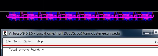
DRC results:
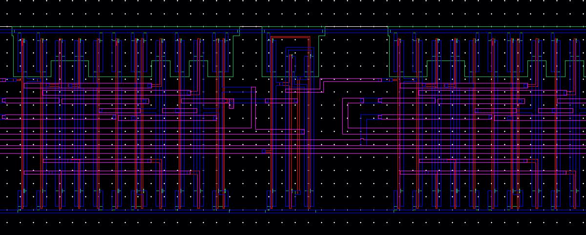
extracted view of the counter
closer look to our extracted view of the counter:
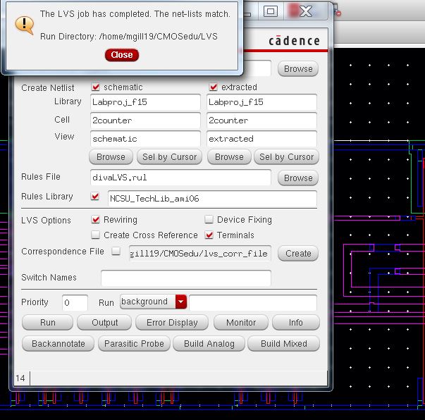
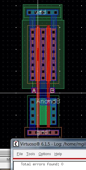
Counter LVS:
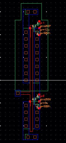
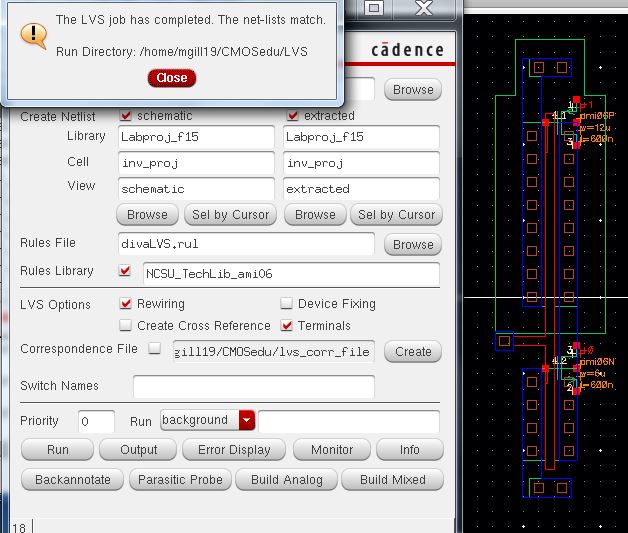
12u/6u Inverter Layout with DRC results :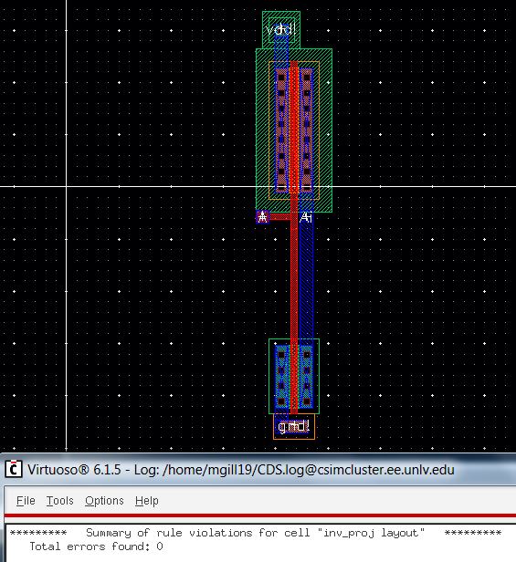
Extracted view :
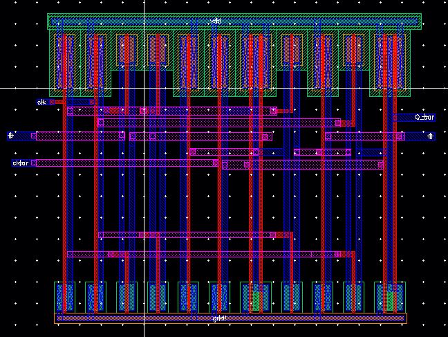
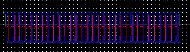
Ring Oscillator Layout:
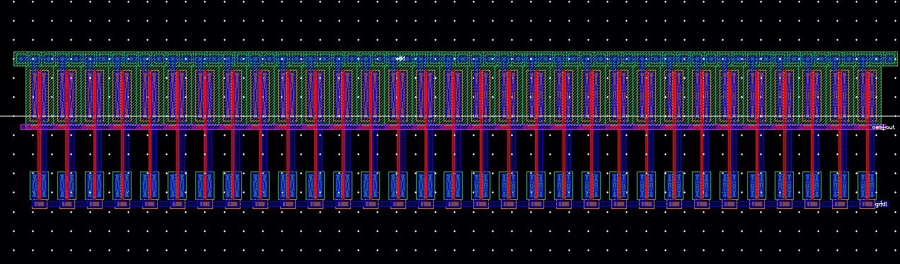
Extracted view of the Ring Oscillator:
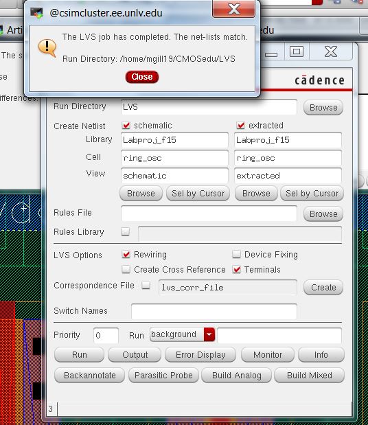
Ring Oscillator LVS:
Now
31_stage ring oscillator with buffer: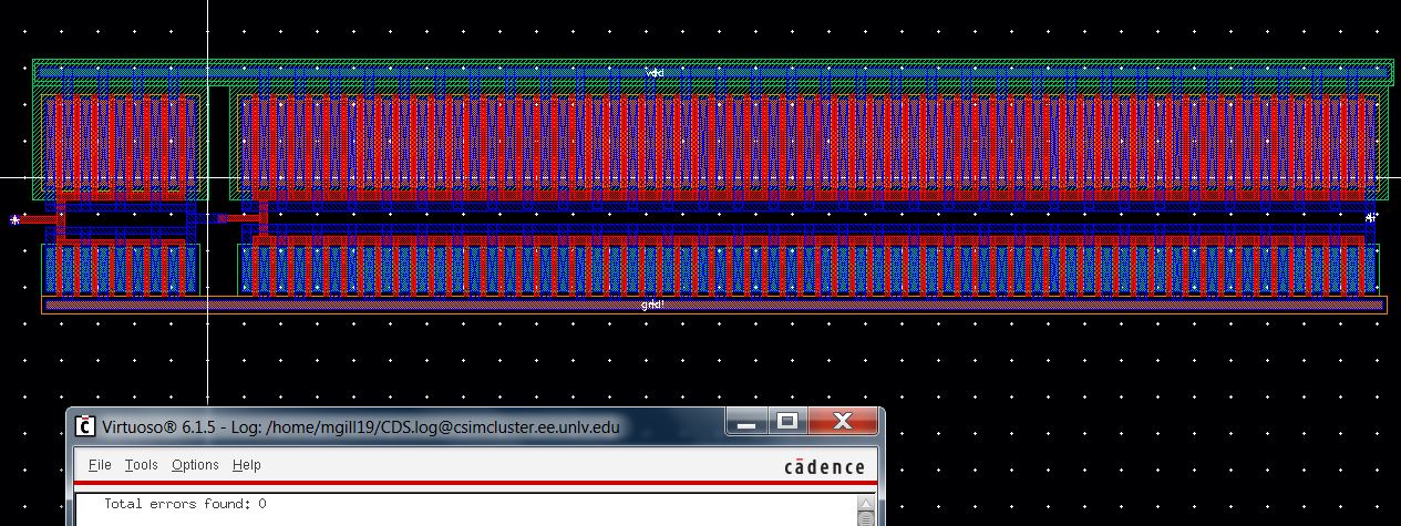
extracted view :
LVS of the 31_stage ring oscillator:
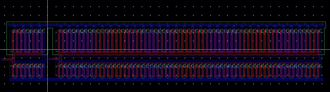
closer view to the extracted view of the ring oscillator:
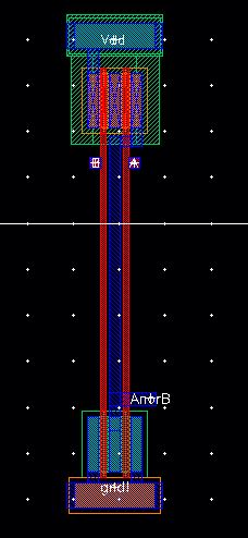
NaND Gate Layout:
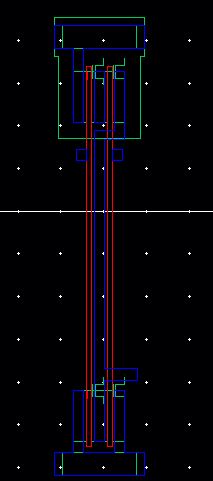
Extracted view of the NAND gate:
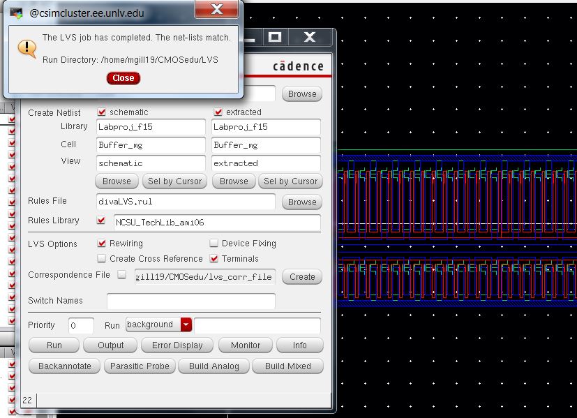
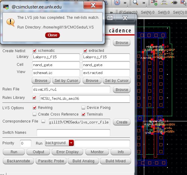
NAND gate LVS:
Nor gate Layout:
Nor gate Extracted view:
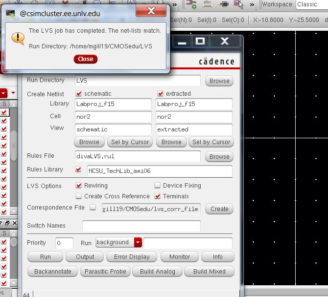
NOR gate LVS:
Buffer Layout:
Extracted view of the Buffer :
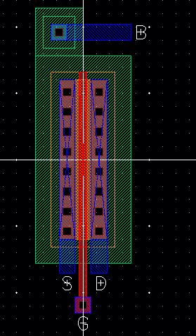
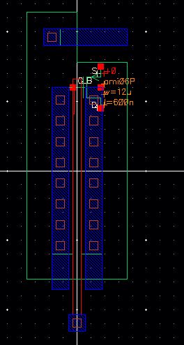
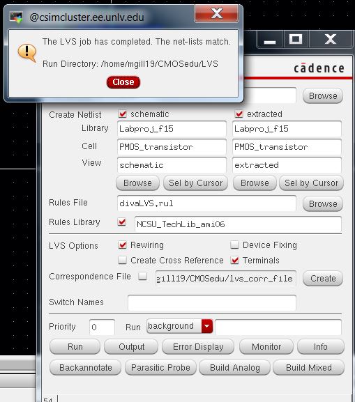
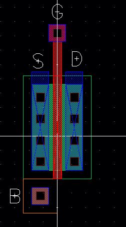
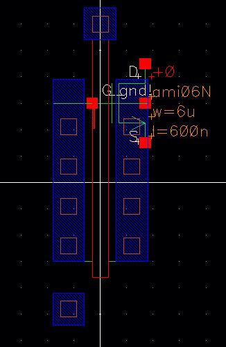
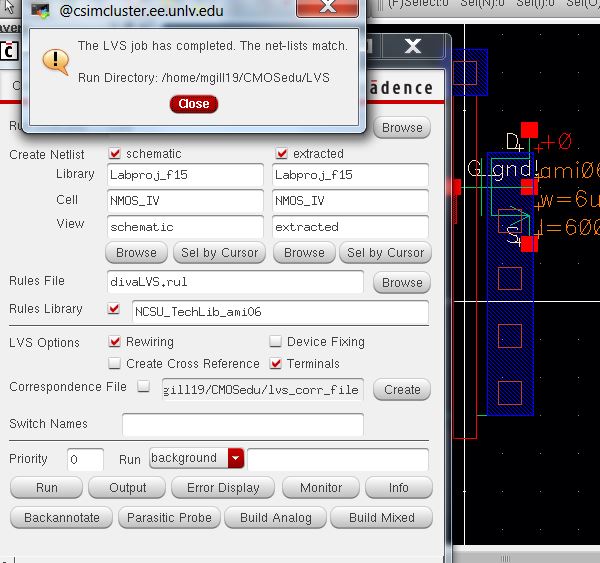
PMOS and NMOS layout and extracted view :
PMOS:
NMOS
Design Directory "Here"
Return to EE 421Labs "Here"
Return to Mari Gilligan Labs "Here"