Lab 2 - ECE 421L
manonej@unlv.nevada.edu
I. Steps taken for the prelab:
After backing up all work from the lab and course, I read through the
entire lab to gain some understanding of the implementation of the ADC
and
DAC.
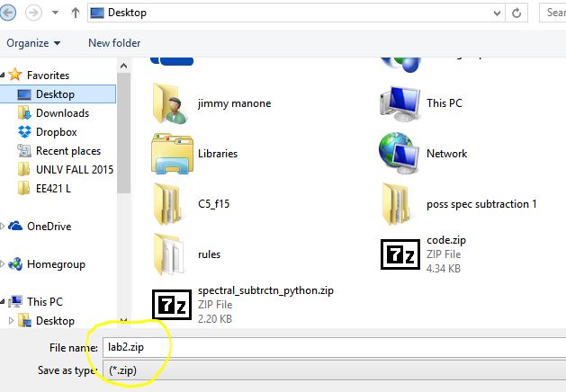
From this point I downloaded lab2.zip to my desktop and extracted the contents:
I then added the following line to the cds.lib file:

I then started Cadence, navigated to lab2 and opened the sim_ideal_ADC_DAC schematic:

I then ran the simulation by selecting Launch (ADE L), Session, Load State, Cell View, and OK:

From this point, the simulation appears like the following:

We can adjust the line thickness by right-clicking on one of the lines and selecting 'Trace Properties':

Solid or dotted lines can be chosen from the middle dropdown menu:

The line thickness can be adjusted using the dropdown menu to the right:

The graph background can be changed as follows by selecting 'graph' from
the main context menu. The following window appears. Select the first
tab 'General' and select the color (or color gradient if preferred):

Changing the background to black and making the traces thicker/solid provides the following result:

II. Provide and discuss different simulation results as related to the ADC and DAC
By changing the values to arbitrary amounts:

We obtain different simulation results than those from the initial
values (Amplitude changed from 2.5V to 500mV, offset from 2.5 to 500mV,
and Frequency changed from 2MHz to 3MHz). The simulation results reflect
these changes in both amplitude and over time:

As the analog voltage is received at the input of the ADC, it's
amplitude values are reflected as a binary representation to the outputs
- with each bit from MSB (most significant bit) to LSB (least
significant bit) being assigned its own output. Depending on the number
of bits (N), the aggregate of the output values will range from 0 to
(2^N -1) for unsigned and -(2^N)/2, ((2^N)/2)-1 for signed
representations.
In this case, the configuration is for 10 bits, so the range of output
in the ADC is 0 to 1023 for unsigned and -512 to 511 for signed
representations.
The inputs to the DAC (arranged in the same configuration as the outputs
of the ADC) are connected to the output of the ADC from the MSB to the
LSB. To convert these binary values to their analog equivalent, each bit
that is a '1' triggers a switch inside the DAC allowing its respective
voltage to be placed in the resistor ladder network (using N-Well
resistors) at its particular location. Voltage division is performed and
the output (Vout) is a direct representation of the result from each
combination of bits in a given time. Vout is similar to Vin (albeit with
the slight digitized stepping effect in the graph) as a result of
signal interpolation and smoothing from the use of the resistor
network/capacitor topology.
III. Explanation of how to determine the LSB and supporting simulation
The formula for determining the minimum voltage change on the input of
the ADC that enables visible changes in the digital code is as follows:
D_0:
1 LSB = (VDD/2^N), where N is the number of bits.
As this is a 10-bit configuration, 2^N = 2^10 = 1024
VDD in the schematic was set to 5V, so the LSB = 5/1024 = 4.88 * 10^-3 or approximately 5mV.
The simulation yields the following:

The voltage of the output (generated
in multiples of 5mV) is less than the voltage of the input. This voltage
difference becomes more prevalent as the number of bits increases.
II. Lab Report
The design of the 10-bit DAC begins with the schematic reflecting a
2R resistor in parallel with an R resistor. The R values are 10k ohms
each.
The schematic is as follows:

From this, we create the symbol and erase the what is not needed:

Now, copy the 10-bit DAC (ideal) to new cell and replace the resistor network with the new symbol

We then turn this into a symbol
(NOTE: When saving, make sure the pins are ordered from B0 to B9), and
delete all of the unnecessary boxes/names:

Deleting the original DAC symbol and placing this symbol into the simulation schematic appears as follows:

After checking and saving the following simulation was ran which was identical to the first simulation:

From this point, we'll test it with a 1K-ohm load on the output to ground:

The simulation is as follows (The output is approximately half that of Vin):

We then introduce a 10pF capacitor and the output is as follows:

The effect on the output involves a smoothing of the signal, thus it appears less jagged. There is also a time
delay introduced of approximately 75ns.
Combining the resistor and capacitor results in a waveform that has the reduced amplitude from the
resistor in combination with the delay (increased to approx 100ns) and smoothing effect of the capacitor:
(modified schematic)

(simulation)

Tying the bits (0-8) to ground and removing the ADC (using pulse) results in the following schematic/simulation:


The delay at 0.3 volts (half of Vout
at 0.6 volts) is approximately 70ns. The calculations 0.7RC =
0.7(10k)(10*10^-12) ~ 70ns, so the waveform verifies the RC delay
calculation.
How to determine the output resistance of the DAC:
Using a 5 bit example, we look at the
bottom of resistor ladder (2R || 2R is just R), then R and R are in
series. Add them and it is again 2R || 2R (The ladder collapses upwards
each time). Do this all the way up, and eventually out solution is R.
See below:

Discuss what happens if the resistance of the switches isn't small compared to R:
If the resistance of switches were
large, it would increase resistance in the ladder (10k series resistors
per bit) causing a further drop in output voltage (See below):

As for every lab, all work is backed up using my Dropbox account in an attempt to minimize the effects of Murphy's Law:
