Lab 2 - EE 421L
Authored
by Brian Kieatiwong
kieatiwo@unlv.nevada.edu
09/14/15
This
lab consists of the understanding and simulation of the ADC and
DAC. It will also consist of designing a 10-bit DAC with different
specifications. This lab will also show the backing up of all lab
work.
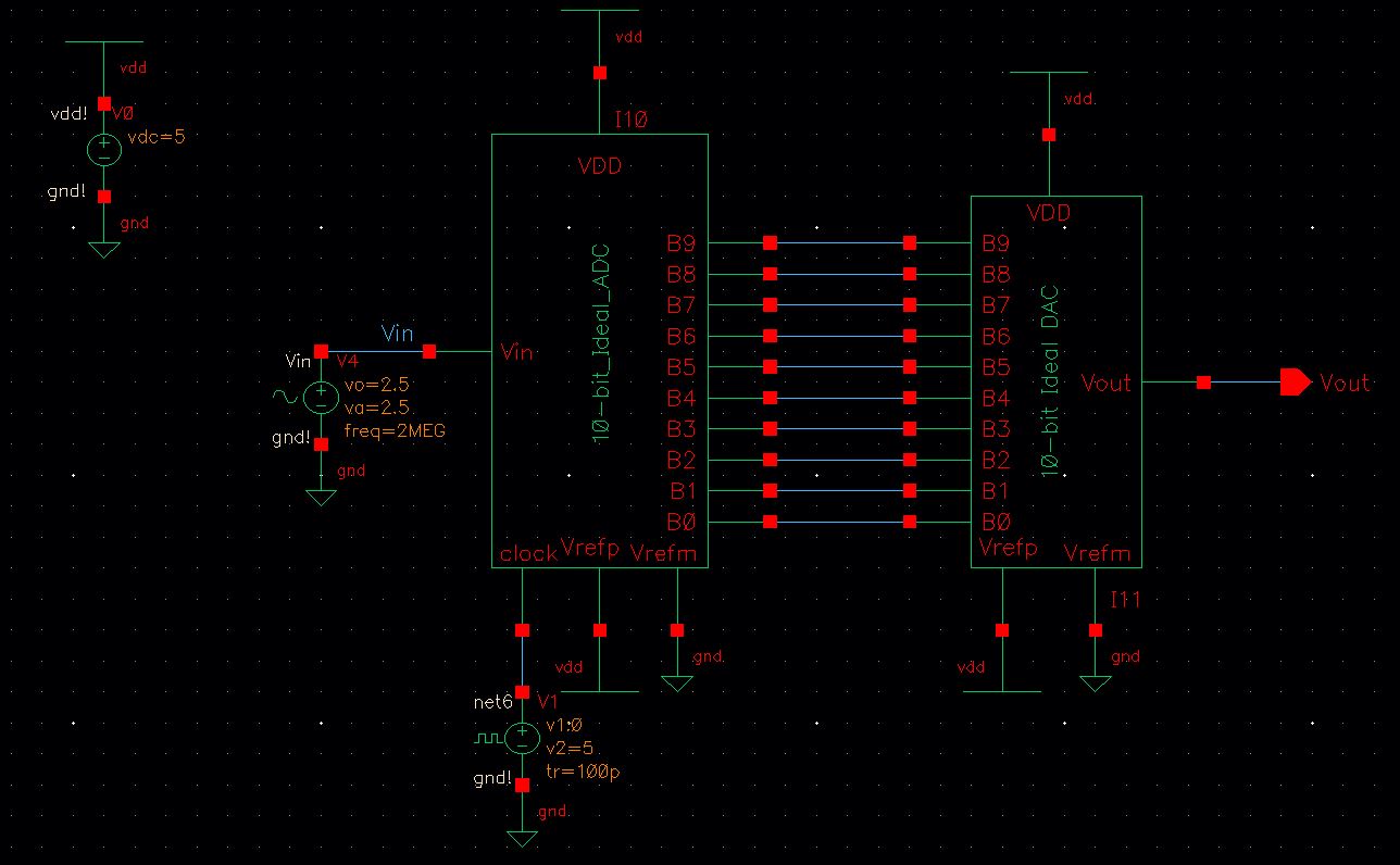
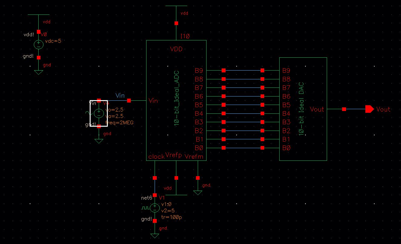
The image above shows the schematic for an ideal ADC-DAC.

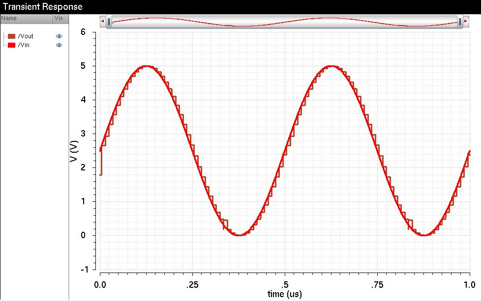
The image above shows the simulation results for the ideal ADC-DAC schematic of the input and output voltages.
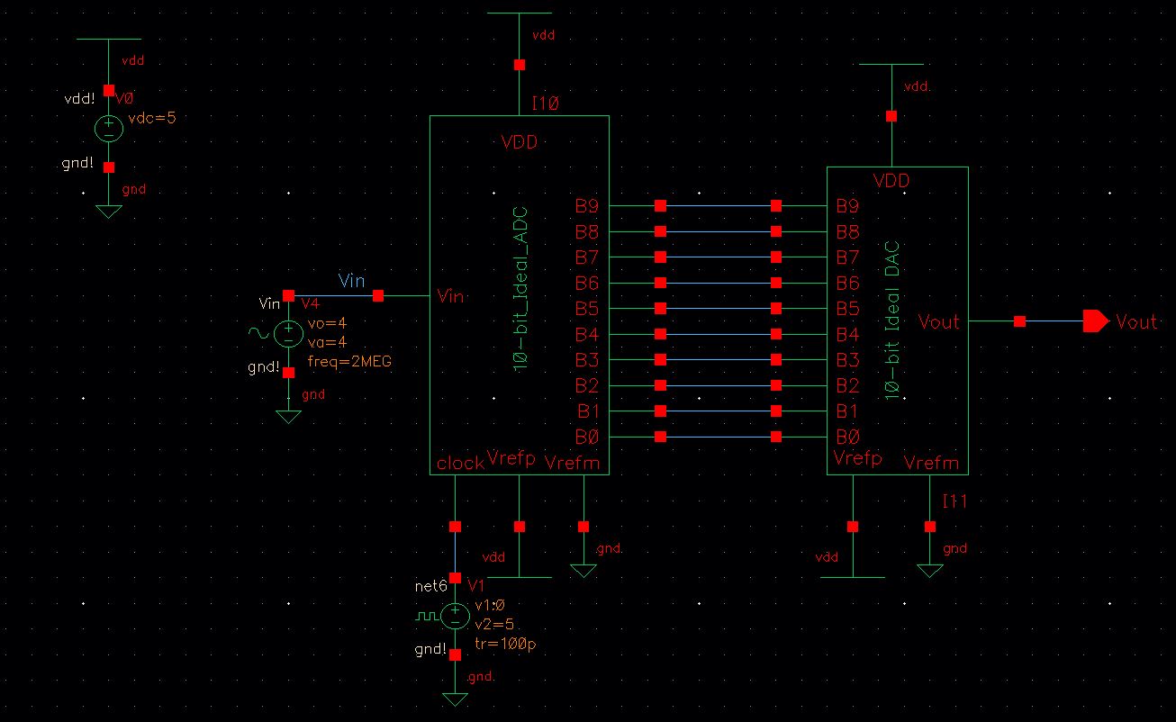
The image above shows the schematic for the ideal ADC-DAC now with an input voltage of 8V rather and the previous 5V.
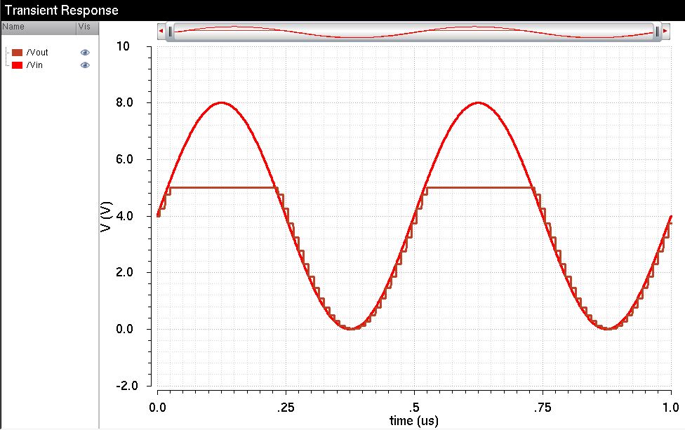
The
image above shows the simulation results for the ideal ADC-DAC
schematic of the input and output voltages. It can be seen that the
output is clipped because it is limited by the VDD of 5V.
To
determiune the last significant bit(LSB) for this particular scenario,
the following criterias should be observed. Since it is a 10 bit
ADC-DAC, the equationisas follows:
2^10 = 1024
LSB = VDD/2^N = 5/1024 = 4.9mV
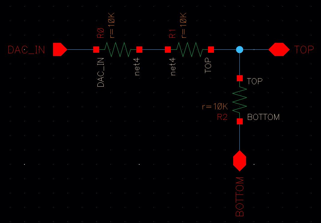
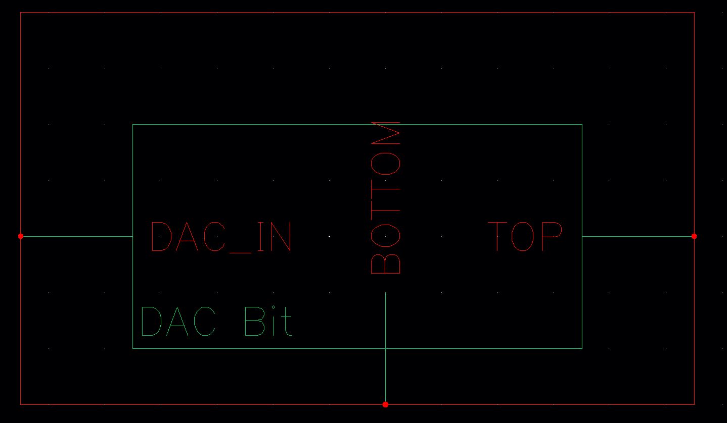
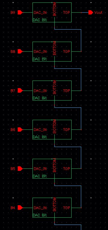
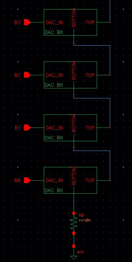
The image above shows the DAC schematic with 10k resistors.
The image above shows the newly created DAC symbol.
The image above shows the schematic for a 10-bit DAC with the newly created DAC symbol.
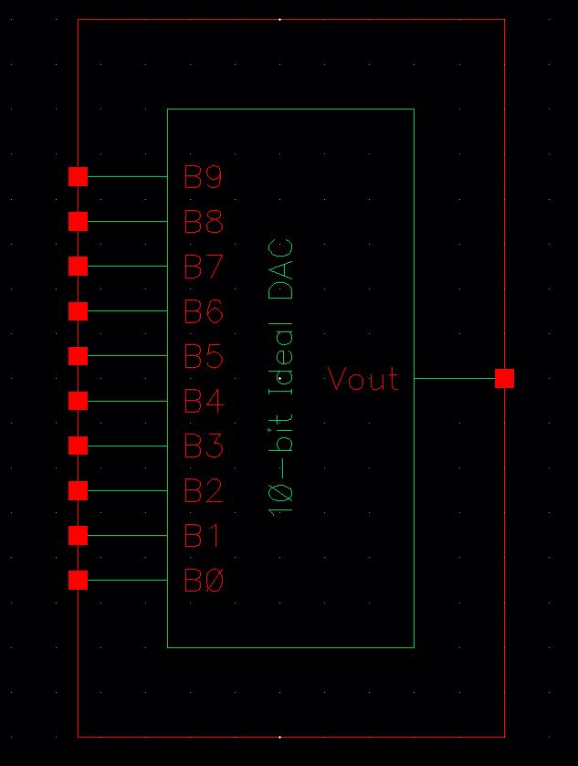
The image above is the newly created 10-bit DAC symbol.
The image above shows the schematic for an ADC-DAC converter with the newly created 10-bit DAC symbol.
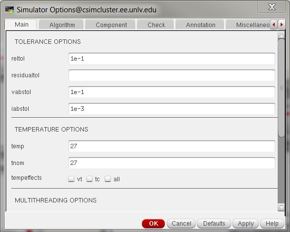
The image above shows the changed parameters for the this particular simulation.
The image above is the simulation results of the ADC-DAC converter schemtaic.
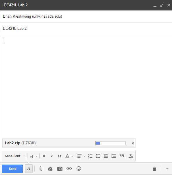
The images above show how Lab 2 work is to be zipped and emailed to myself for backup.
Return to EE421L Labs