Lab 7 - ECE 421L
Authored
by Jesse Horsman,
11/2/2015
horsman@unlv.nevada.edu
Lab
description:
Using buses and arrays in the design of word inverters, muxes, and high-speed adders
Creating an array (4 bit) of an inverter:

With its accompining simulation:

As
you can see from the simulation, the bigger the capacitive load, the
more delay to changes in voltage. Comparing out<0> (no
load) and out<1> (the largest load of 500f), out<1> takes
approximatly 2ns more to reach ground when power is supplied by input.
The rise time is even worse for the heavier loads, as
out<1> takes almost 6ns longer than out<0>!
Create schematics and symbols for an 8-bit input/output array of: NAND, NOR, AND, inverter, and OR gates.
Provide a few simulation examples using these gates.
8-bit NAND gate:

The NAND's simulation:

8 bit NOR gate:

NOR's simulation:

8-bit OR gate:

OR's simulation:

8-bit AND gate:

AND's Simulation:

8-bit inverter:

Inverter's sim:
Simulate the operation of a 2-to-1 DEMUX/MUX:
Circuit of the MUX:

Simulation of the MUX:

As
the simulation shows, you can control which input is sent to the output
by controling the S and Si signals. As long as Si is inverse of
S, having S = 1 will cause the output to yeild input from A, and when S
= 0, output will be the input from B. This works due to the
properties of the NMOS and PMOS devices. The S and Si control the
voltage to the gates, thus controling the output of the inputs A and B.
Both PMOS and NMOS are needed because they cover for each others
weakness (gets around the volage drop that occurs in one end of the
spectrum for each device). A result of only using one of the
devices instead of both is evedence shown above in the sim, when S and
Si end up equal, and the output voltage losses a few volts from the
input.
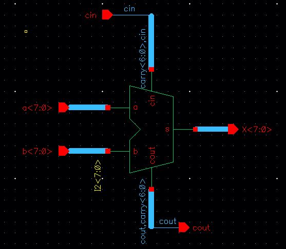
Create an 8-bit wide word 2-to-1 DEMUX/MUX schematic and symbol:
2-to-1 DEMUX/MUX simulation:

Finally, draft the schematic of the full-adder seen in Fig. 12.20 using 6u/0.6u devices (both PMOS and NMOS).
Use this symbol to draft an 8-bit adder schematic and symbol.


Simulation of the operation of my 8-bit adder.

Layout of FullAdder with DVS:
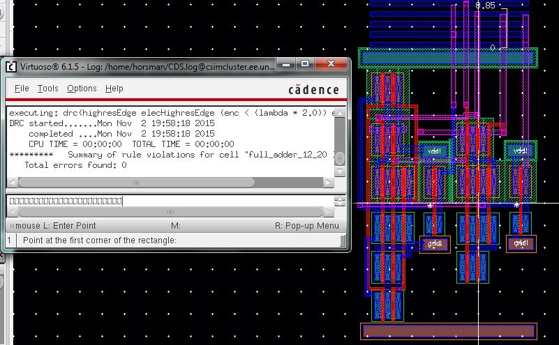
Notice
that because of delay, you can see some glitches more evedent with the
later outputs and cout, specifically around time = 125ns where the
delay is so bad, it looks like it may been a result from an addition
and not just a proprogation delay. This is usually avoided either
by using look ahead adders (this is a ripple adder) or using
capacitors. This can be seen having good results from the sim of
the NOR gate, where the 500f capacitive load was able to midigate the
consequence of delay to be only somewhat detectable. So though
Capacitors slow operation, they help cover up glitches that can give
false results.
Return to My EE421L Labs