Lab 3 - ECE 421L
Layout of the 10-bit DAC that was designed in Lab 2.

In order to determine the minimum length and width of the 10k resistor, we need to reference the C5 process design rules on the minimum width of n-well. In this case, the minimum width is 12-lambda.
So 12*(300nm) = 3.6 um.

We chose a width of 4.5um. We determine the length by the formula L/W * P/R. So L = 10k/800 ohms/sq * 4.5um = 56.1. We enter the dimensions as shown below in order to contruct the resistor.

The length/width can be verified by measuring the layout with the ruler command (k).

Our DAC layout is based off of this design presented to us in Lab2.

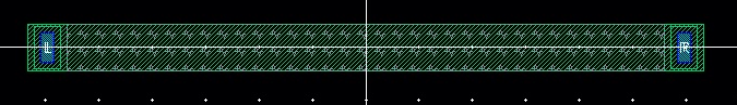
Design one bit of the DAC consisting of two 10k resistors in parallel with a single 10k resistor. We first layout 3 10k resistors on top of each other, with metal 1 extensions.

Then we layout 1-bit of the DAC by adding metal 2 in order to connect the resistors and the proper pins.

The MSB is modified to have the Vout pin.

The LSB is modified to have an extra resistor before gnd and to include the gnd! pin itself.

The final layout should look something like this.

Now we verify that our layout is correct by running a DRC.

Backup:
Cadence files and lab report are automatically backed up in my Dropbox folder.


The cadence files can be found here: Lab3.zip